How to Design PCB in Altium/KiCad/Eagle: Complete Step-by-Step Guide
Designing your first printed circuit board can feel overwhelming with dozens of software options available. Three tools dominate the PCB…
How to Design PCB in Altium/KiCad/Eagle: Complete Step-by-Step Guide
Designing your first printed circuit board can feel overwhelming with dozens of software options available. Three tools dominate the PCB design landscape: Altium Designer for professionals, KiCad for open-source enthusiasts, and Eagle for hobbyists and startups. This comprehensive guide walks you through designing PCBs in all three platforms, comparing their strengths, and revealing how to avoid costly manufacturing mistakes.
Choosing the Right PCB Design Software
Altium Designer: The Professional Standard
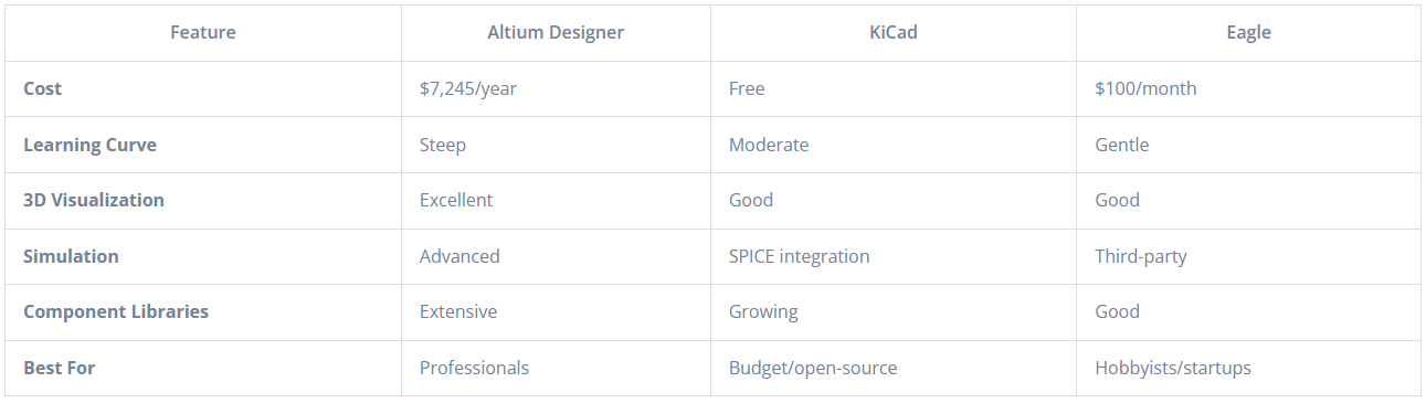
Best For: Complex professional designs, high-speed circuits, enterprise projects Cost: $7,245/year (professional license) Strengths: Advanced simulation, 3D visualization, robust design rule checking, extensive component libraries Learning Curve: Steep but powerful
KiCad: The Open-Source Champion
Best For: Budget-conscious designers, open-source projects, learning PCB design Cost: Completely free Strengths: Professional features at zero cost, growing community, cross-platform (Windows/Mac/Linux) Learning Curve: Moderate, excellent tutorials available
Eagle (Autodesk Fusion 360)
Best For: Small to medium projects, hobbyists, startups Cost: $100/month (standard), free for hobbyists (limited features) Strengths: Intuitive interface, good component libraries, Fusion 360 integration Learning Curve: Gentle, user-friendly
Complete PCB Design Workflow (All Software)
Regardless of which tool you choose, PCB design follows these fundamental steps:
Step 1: Create Project and Schematic
Altium Designer:
- File → New → Project
- Right-click project → Add New to Project → Schematic
- Set page size (A4/A3) based on circuit complexity
- Configure grid settings (typically 100 mil for schematics)
KiCad:
- File → New Project
- Open Schematic Editor (*.kicad_sch file)
- The interface opens with hierarchical block structure
- Configure preferences: Edit → Preferences → Schematic Editor
Eagle:
- File → New → Project
- Right-click → New → Schematic
- Set drawing size and grid parameters
- Eagle auto-saves, reducing data loss risk
Step 2: Place Components
Component Libraries: All three software packages include extensive component libraries. Access them through:
- Altium: Panels → Components (or press ‘P’)
- KiCad: Add Symbol tool, browse integrated libraries
- Eagle: Library Manager → Use (enable relevant libraries)
Best Practices:
- Search by manufacturer part number for accuracy
- Verify footprint matches your component’s physical package
- Create custom symbols/footprints only when necessary
- Organize components logically (power, microcontroller, peripherals)
Step 3: Create Schematic Connections
Wiring Components:
- Altium: Place → Wire (or press ‘W’), click to start/end connections
- KiCad: Right toolbar → Wire tool, connect symbol pins
- Eagle: Draw → Net tool, click between component pins
Naming Nets: Give meaningful names to important signals (e.g., “VCC_3V3”, “SPI_MOSI”, “LED_STATUS”) for easier debugging and routing.
Power and Ground:
- Use power symbols (GND, VCC, +5V) instead of drawing wires everywhere
- This reduces schematic clutter and improves readability
Step 4: Run Electrical Rules Check (ERC)
Critical Validation:
- Altium: Tools → ERC, review warnings/errors
- KiCad: Inspect → Electrical Rules Checker
- Eagle: Tools → ERC, address all issues
Common ERC Errors:
- Unconnected pins (floating inputs)
- Power pins not connected
- Multiple drivers on single net
- Missing net names
Fix all errors before proceeding to layout. ERC catches mistakes that cause non-functional boards.
Step 5: Generate Netlist and Import to PCB Editor
Synchronizing Schematic to Layout:
Altium: Design → Update PCB Document, select design changes, Execute Changes
KiCad:
- Enable Ratsnest button (left toolbar)
- Tools → Update PCB from Schematic
- Select “Re-link footprints” option
- Click Update PCB
Eagle: Automatically synchronized — switch between schematic and board views seamlessly using the ULP (User Language Program) scripts
Step 6: Define Board Outline
Setting Board Dimensions:
- Altium: Design → Board Shape → Define from selected objects
- KiCad: Edge.Cuts layer, draw outline with line/arc tools
- Eagle: Dimension layer, draw board outline
Standard Sizes: Common board sizes include 50×50mm, 100×100mm (fits standard panels), or custom dimensions matching your enclosure.
Step 7: Place Components Strategically
Component Placement Strategy:
High-Speed Components: Microcontrollers, FPGAs — place centrally to minimize trace lengths to all peripherals.
Analog Circuits: Group together, separate from noisy digital sections.
Power Circuits: Place regulators near board edge for heat dissipation, add thermal vias.
Connectors: Position at board edges for accessibility.
Decoupling Capacitors: Place within 0.25″ (6mm) of IC power pins.
All Software Support:
- Drag components manually
- Auto-arrange tools (limited effectiveness)
- 3D visualization to check mechanical fit
- Ratsnest (airwires) shows optimal placement
Step 8: Configure Design Rules
Critical Design Rules (adjust based on your manufacturer):
**Trace Width**: Minimum 6–10 mils (0.15–0.25mm) for signals, wider for power (calculate based on current)
Trace Spacing: Minimum 6–8 mils (0.15–0.2mm) clearance
Via Size: 0.3mm drill, 0.6mm pad typical
Copper to Edge: Minimum 10–20 mils (0.25–0.5mm)
Setting Rules:
- Altium: Design → Rules, configure categories
- KiCad: File → Board Setup → Design Rules
- Eagle: DRC button → Design Rules dialog
Step 9: Route Traces
Manual Routing: All three tools offer interactive routing with design rule checking:
Altium: Route → Interactive Routing (or press ‘TAB’ for options)
KiCad: Three routing modes — Highlight collisions, Shove, Walkaround
Eagle: Route tool with automatic obstacle avoidance
Routing Best Practices:
- Route critical signals first (clocks, high-speed data)
- Keep traces short and direct
- Use 45° angles, avoid 90° bends (though modern boards tolerate 90°)
- Match lengths for differential pairs and parallel buses
- Maintain 3× trace width spacing between high-speed signals
- Use ground plane fill for return paths
Auto-Routing: All three support auto-routing, but manual routing produces superior results for critical signals. Use auto-routing only for simple boards or non-critical traces.
Step 10: Add Copper Pours (Ground/Power Planes)
Polygon/Zone Fills:
- Altium: Place → Polygon Pour, set net (GND/VCC)
- KiCad: Add Filled Zone tool, assign to ground or power net
- Eagle: Polygon tool, name GND or VCC, ratsnest to fill
Ground Plane Benefits:
- Low-impedance return path for signals
- EMI shielding
- Heat dissipation
- Simpler routing (reduces trace count)
Step 11: Run Design Rule Check (DRC)
Final Validation:
- Altium: Tools → Design Rule Check
- KiCad: Inspect → Design Rules Checker
- Eagle: DRC button, review errors
Fix All Violations before manufacturing:
- Clearance errors (traces/pads too close)
- Unrouted connections
- Silkscreen over pads
- Copper to edge clearance
Step 12: Generate Manufacturing Files
**Gerber Files** (industry standard):
Altium: File → Fabrication Outputs → Gerber Files
- Include all copper layers, solder mask, silkscreen, drill files
KiCad: File → Plot
- Select all layers, generate drill files separately
Eagle: CAM Processor → Use CAM job file
- Standard Gerber RS-274X format
Required Files:
- Copper layers (.GTL, .GBL, etc.)
- Solder mask top/bottom (.GTS, .GBS)
- Silkscreen top/bottom (.GTO, .GBO)
- Drill files (.TXT or .DRL)
- Board outline (*.GKO)
Additional Documentation:
- Bill of Materials (BOM) with manufacturer part numbers
- Assembly drawings showing component locations
- Pick-and-place files (if ordering assembly)
Comparing the Three Software Platforms
https://morepcb.com/how-to-design-pcb-altium-kicad-eagle-complete-guide
Common PCB Design Mistakes to Avoid
1. Inadequate Trace Width: Calculate based on current requirements using IPC-2221 standards.
2. Poor Decoupling: Place capacitors close to IC power pins, not scattered randomly.
3. Ground Plane Splits: Never split ground plane under high-speed traces.
4. Ignoring Thermal Relief: Add thermal relief to ground plane connections for easier soldering.
5. Missing Design Rule Checks: Always run ERC and DRC before manufacturing.
Choosing a Quality PCB Manufacturer
Even perfectly designed PCBs fail if manufacturing introduces defects. Select manufacturers carefully:
Essential Qualifications:
- ISO 9001, IPC standards certification
- DFM (Design for Manufacturing) review service
- Gerber file verification before production
- Electrical testing (flying probe or fixture)
- AOI (Automated Optical Inspection)
Why MorePCB Ensures Manufacturing Success
When your PCB design is complete, MorePCB provides manufacturing expertise ensuring your Altium, KiCad, or Eagle designs become reliable products.
Accepts All Design Formats:
- Native Altium files (.PcbDoc)
- KiCad exports (.kicad_pcb + Gerbers)
- Eagle files (.brd) or standard Gerbers
- Automatic Gerber validation
Proactive DFM Review: MorePCB’s engineering team reviews every design:
- Identifies potential manufacturing issues
- Suggests improvements for reliability
- Optimizes for cost-effective production
- Prevents common first-time designer mistakes
Quality Manufacturing:
- ISO 9001, IATF 16949 certified
- 1–30+ layer capability
- Fine-line technology (3/3 mil trace/space)
- Controlled impedance options
- Multiple surface finishes
Flexible Volumes:
- Prototypes (1–10 boards) to validate designs
- Small batch (10–100) for testing
- Production volumes with consistent quality
- No minimum order quantity
Complete Support:
- English-speaking project managers
- Technical consultation for complex designs
- Component sourcing assistance
- Global shipping
By partnering with MorePCB, you ensure designs from any software platform — Altium, KiCad, or Eagle — translate into manufacturable, high-quality PCBs.
Frequently Asked Questions
Q: Which PCB design software should beginners start with? A: KiCad offers the best entry point — completely free with professional features and excellent tutorials. Eagle provides easier initial learning but requires paid subscription.
Q: Can I switch between PCB design software? A: Yes, but with effort. All three export standard Gerber files for manufacturing. Importing native files between platforms requires conversion (some data loss possible).
Q: How long does it take to learn PCB design? A: Basic proficiency: 2–4 weeks for simple designs. Advanced features: 3–6 months. Complex professional work: 6–12 months of regular practice.
Q: Do I need Altium’s expensive license as a hobbyist? A: No. KiCad provides 90% of Altium’s functionality free. Altium’s advantages (advanced simulation, enterprise features) matter most for complex professional work.
Q: Can I design high-speed PCBs in KiCad? A: Yes. KiCad supports controlled impedance, differential pairs, and advanced routing. For extremely complex high-speed designs (>10 GHz), Altium’s simulation capabilities provide advantages.
Q: What file format do PCB manufacturers prefer? A: Standard Gerber RS-274X files accepted universally. Some manufacturers like MorePCB also accept native files from Altium, KiCad, and Eagle for better accuracy.
메타데이터
- post_id
- a4c4ca9fed19
- slug
- how-to-design-pcb-in-altium-kicad-eagle-complete-step-by-step-guide-a4c4ca9fed19
- url
- https://medium.com/@aa.suryanegara2/how-to-design-pcb-in-altium-kicad-eagle-complete-step-by-step-guide-a4c4ca9fed19
- canonical_url
- https://medium.com/@aa.suryanegara2/how-to-design-pcb-in-altium-kicad-eagle-complete-step-by-step-guide-a4c4ca9fed19
- author_url
- https://medium.com/@aa.suryanegara2
- status
- ok
- fetched_at
- 2026-07-15 14:59:38