Building My First Custom PCB:
A Cybersecurity Researcher’s Journey from Breadboards to Real Hardware
Ai
Building My First Custom PCB:
A Cybersecurity Researcher’s Journey from Breadboards to Real Hardware
***FREE ACCESS FOR EVERYONE***
How an open-source hardware project inspired me to design my first custom wireless research platform — and why this is just the beginning…
“One day I’ll build my own PCB……….”
I’ve been telling myself that for almost two years.
Like most people getting into hardware, I started with development boards. An ESP32, a breadboard, jumper wires, and whatever sensors I could get my hands on. It was enough to learn, experiment, and break things. Every project taught me something new, but they all had one thing in common — they always looked unfinished
Every project eventually became another breadboard sitting on my desk, waiting to be dismantled for the next idea.
And every time I watched someone show off a beautifully designed custom PCB or a handheld hacker gadget on YouTube, I had the exact same thought.
“One day…”
Turns out, “one day” never arrives.
At some point, you simply have to begin.
Who Am I?
I’m Satyam Pathania, although most people online know me as 0xDiddy.
I’m a self-taught cybersecurity researcher, technical writer, and someone who’s constantly distracted by interesting hardware.
Most of my work revolves around offensive security, vulnerability research, bug bounty hunting, writing technical articles, and collaborating with cybersecurity companies to explain complex topics in a way that’s easier to understand. Somewhere along the way, I also developed an unhealthy habit of collecting ESP32 boards and hacker gadgets that promised to teach me “just one more thing.”
Recently, though, something changed…..
Instead of simply reviewing hardware or using development boards for quick experiments, I started becoming curious about what happens underneath. How are these devices actually designed? Why are certain components chosen? How does an idea become a PCB that fits in the palm of your hand?
The more questions I asked, the deeper I fell into the world of embedded systems, wireless research, and custom electronics.
This article is the beginning of that journey.
Every Breadboard Project Eventually Hits a Wall
If you’ve built anything with an ESP32 before, you’ll probably relate to this.
Breadboards are amazing for prototyping. They let you test ideas quickly, move components around, and learn without worrying about making permanent mistakes.
But eventually you reach a point where the project works… and that’s it.
The wiring becomes messy.
The jumper cables start falling out.
You hesitate to move the project because one loose wire means another debugging session.
The project technically works, but it never feels complete.
That was exactly where I found myself.
I didn’t want another prototype.
I wanted to build something that actually felt like a finished piece of hardware.
The Tech Hole Started With One ESP32
Funny enough, this project wasn’t planned.
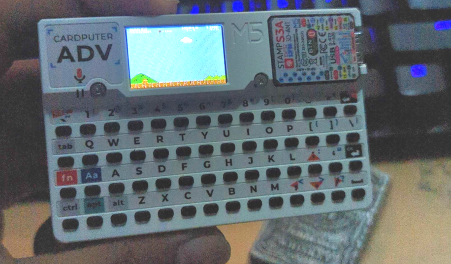
A few months ago I started spending more time experimenting with ESP32-based devices like the M5Stack Cardputer ADV. I was supposed to review the hardware, write about it, and move on to the next project.
Instead, I ended up flashing custom firmware, exploring wireless protocols, understanding BLE communication, and learning how much capability could fit inside such a tiny device.
That naturally led me toward LoRa, RF experimentation, IoT security, and portable wireless tools.
While exploring the community around these projects, I came across nRFBox, an open-source wireless research platform created by CiferTech.
What impressed me wasn’t just the finished device.
It was everything behind it.
The complete documentation.
The schematics.
The PCB files.
The Bill of Materials.
The firmware.
The fact that someone had built something useful and then shared every detail so others could learn from it.
That completely changed how I looked at hardware.
For the first time, designing a PCB didn’t feel like something reserved exclusively for electrical engineers.
It felt achievable.
Project 0xD: Building My First Wireless Research Platform
Inspired by nRFBox, I decided to begin my own project.
Not a clone.
Not a commercial product.
Not something I’m planning to sell.
Just a platform that allows me to understand hardware design while creating something that reflects my own workflow and personality.
At the moment, I’m calling it Project 0xDiddy
The idea is to build a compact wireless research platform based around the ESP32-S3, using the open-source project as a learning foundation while gradually customising both the hardware and the aesthetics.
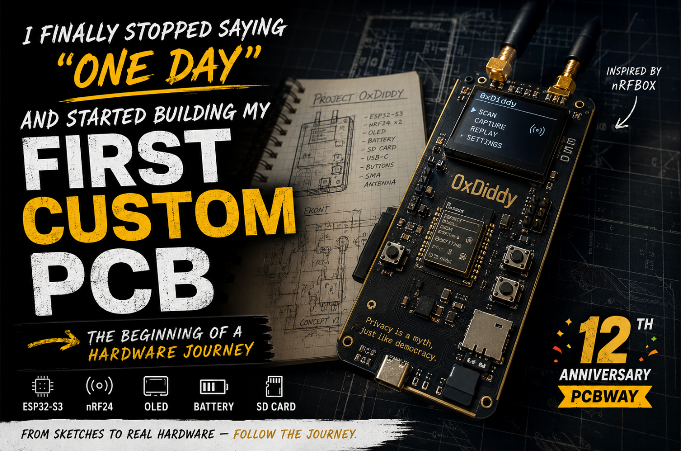
The first revision is planned to include an ESP32-S3 for Wi-Fi and Bluetooth communication, dual or possibly triple nRF24L01 modules for 2.4 GHz wireless experimentation, a 0.96-inch OLED display, a rechargeable lithium battery, USB-C programming and charging, an SD card slot for firmware and logging, physical navigation buttons, and external SMA antennas.
Visually, I already know exactly how I want it to look…
A black PCB.
ENIG gold finish.
White silkscreen.
A clean acrylic enclosure.
Minimal branding.
And one sentence printed on the back that perfectly sums up my sense of humour.
Privacy is a myth, just like democracy.
Will it work the first time?
Probably not.
Will I make mistakes?
Absolutely.
That’s exactly why I’m documenting everything.
Learning PCB Design Is More Than Drawing a Circuit
Before starting this project, I thought PCB design was mostly about connecting components together.
The more I read, the more I realised how wrong I was.
There are schematics that define how everything connects electrically.
PCB layouts that determine where every component sits.
Gerber files that tell manufacturers how to fabricate the board.
Bills of Materials that list every resistor, capacitor, connector, and integrated circuit.
Pick-and-place files that guide assembly machines.
Then there are engineering reviews, manufacturing tolerances, PCB stack-ups, trace widths, and countless design decisions that most of us never think about when we buy a finished product….
Two weeks ago, I barely knew what half of those terms meant.
Today, they’re becoming part of my daily reading.
That’s one of the reasons I wanted to document this journey publicly.
Because I know there are countless software engineers, cybersecurity researchers, and makers who are standing exactly where I was — not knowing where to begin.
From KiCad to Manufacturing: Turning an Idea into Real Hardware
Designing a PCB is only half the journey.
Eventually, your design has to leave the screen.
It has to be reviewed, manufactured, assembled, and tested before it becomes something you can actually hold in your hands.
Since this is my very first custom PCB, I wanted to understand that entire workflow instead of stopping at the design stage.
That naturally led me to PCBWay.
Rather than simply ordering a board, I’m looking forward to learning about PCB fabrication, PCB assembly (PCBA), engineering feedback, manufacturing constraints, and everything else that happens between uploading a design and receiving a finished board.
As I was planning this project, I also discovered that PCBWay is celebrating its 12th Anniversary this month. The timing honestly couldn’t have been better. After spending years saying “I’ll build my own PCB someday,” it felt like the perfect opportunity to finally stop postponing the idea and actually commit to building it.
If you’ve been thinking about designing your own custom PCB or experimenting with your first hardware project, their anniversary campaign is worth checking out. Whether you’re a student, hobbyist, or someone who’s simply curious about electronics, it might be the little push you need to finally start building.

https://www.pcbway.com/activity/anniversary12th.html?activity=Join02
This Is More Than One PCB
Although this article is centred around a single project, I don’t see it ending there.
If everything goes well, this will become the first device in a much larger collection of cybersecurity and hardware projects.
I want to build a LoRa communication platform.
A cyberdeck.
Custom ESP32 tools.
Portable RF research devices.
Hardware designed specifically for learning, experimentation, and cybersecurity research.
More importantly, I want to document every success and every failure along the way.
Not polished marketing videos.
Not perfect project showcases.
The real process.
The late-night debugging.
The failed revisions.
The tiny mistakes that somehow take six hours to figure out.
Because that’s the part nobody usually shows.
What’s Coming in Part 2?
Right now, this project exists as sketches, research notes, GitHub repositories, and way too many browser tabs.
The real work starts next.
In the next article, I’ll dive into the original open-source hardware, explain why each component was chosen, walk through the PCB design process, share the changes I’m planning to make, and document everything that happens before the design is finally sent for manufacturing.
If you’re a hardware engineer, PCB designer, or maker, I’d genuinely love to hear your advice before I send the first revision for fabrication.
And if you’re someone who’s been putting off that “one day” project, maybe this series will convince you to finally begin.
Because if there’s one thing I’ve learned already, it’s this:
You don’t need to know everything before you start.
You just need to be curious enough to take the first step.
See you in Part 2.
메타데이터
- post_id
- 03f523ee2a33
- slug
- building-my-first-custom-pcb-03f523ee2a33
- url
- https://radiohackers.com/building-my-first-custom-pcb-03f523ee2a33
- canonical_url
- https://radiohackers.com/building-my-first-custom-pcb-03f523ee2a33
- author_url
- https://medium.com/@SatyamPathania
- status
- ok
- fetched_at
- 2026-07-11 10:44:35