5 Common Rigid-Flex PCB Design Pitfalls (And How to Avoid Them)
Rigid-Flex PCBs are increasingly appearing in wearables, medical sensors, aerospace, and foldable consumer electronics. They combine the…
5 Common Rigid-Flex PCB Design Pitfalls (And How to Avoid Them)
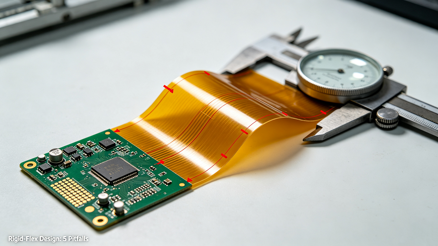
Rigid-Flex PCBs are increasingly appearing in wearables, medical sensors, aerospace, and foldable consumer electronics. They combine the support and high-density interconnect capability of rigid boards with the bending and 3D assembly advantages of flexible circuits.
But many hardware engineers designing rigid-flex for the first time fall into the same traps — from insufficient bend radius to asymmetric stackups, from coverlay opening errors to stiffener design mistakes. These can lead to assembly difficulties or even cracked flexible circuits.
This article shares five easily overlooked design details and provides an actionable checklist to help you avoid these pitfalls.
Pitfall 1: Bend Radius Too Small in Flexible Areas
Symptom: Cracks in the flexible circuit after repeated bending, especially in dynamic flex applications.
Cause: Copper foil and polyimide substrates have fatigue limits. When the bend radius is smaller than recommended, the copper foil experiences compression on the inner side and tension on the outer side, causing stress fractures after hundreds of cycles.
Correct approach:
- Static bending (assembled once, no repeated flex): Bend radius ≥ 3× total flex thickness. Minimum recommended: 1.5mm.
- Dynamic bending (repeated flex in use): Bend radius ≥ 10× total flex thickness. Typical dynamic applications require radius ≥ 5mm.
- Avoid vias in the bending area: Vias are stress concentration points that dramatically reduce flex life.
- Copper orientation: The bend axis should be perpendicular to the copper rolling direction.
Pitfall 2: Asymmetric Stackup Between Rigid and Flexible Sections
Symptom: Severe warpage after reflow soldering, or delamination between rigid and flexible regions.
Cause: Rigid sections are typically laminated with multiple layers of copper-clad laminate and prepreg, while flexible sections consist only of polyimide substrate and copper foil. If the rigid sections on both sides are asymmetric in thickness, copper distribution, or layer count, they shrink differently during lamination.
Correct approach:
- Symmetric design: Rigid sections should be as symmetrical as possible about the center layer. For multilayer rigid-flex, ensure the flex layers are positioned in the middle of the stackup.
- Control dielectric thickness: Use the same thickness and type of prepreg on both sides.
- Match copper coverage: Keep copper coverage on the top and bottom rigid sections as close as possible.
Pitfall 3: Insufficient Coverlay Opening Clearance
Symptom: Coverlay lifting at pad edges during SMT, or solder wicking underneath the coverlay.
Cause: Coverlay (flexible solder mask) is opened to expose pads. If the opening edge is too close to the pad copper boundary (typically < 0.2mm), the coverlay shrinks or peels at high temperatures.
Correct approach:
- Coverlay opening size: 0.2‑0.3mm larger than the pad on each side, ensuring full pad exposure with adequate coverlay adhesion.
- Avoid opening across multiple nets: Don’t expose pads of different nets in the same opening.
- For fine‑pitch (≤0.5mm) QFN or BGA pads: Use photoimageable solder mask instead of coverlay for more precise openings.
Pitfall 4: Improper Stiffener Design Causing Placement Issues or Stress Concentration
Symptom: Board deformation during placement at connector or heavy component locations, or cracks at the rigid-flex interface.
Cause: Stiffeners (PI or FR-4 material bonded to the flex section) add local thickness for support. Improper thickness, material, or bonding area creates thermal expansion mismatch or abrupt rigidity changes.
Correct approach:
- Thickness selection: Stiffener thickness should be close to the total thickness of the adjacent rigid section. Common thicknesses: 0.1mm, 0.2mm, 0.3mm.
- Transition zone: Stiffener edges should be located within the flex section, at least 3‑5mm from the rigid-flex interface.
- Openings in stiffener: If the stiffener covers the bending area, it must be opened (notched) there.
- Material matching: For multiple reflow cycles, FR‑4 stiffeners are more heat-resistant than PI.
Pitfall 5: Ignoring Stress Relief and Via Placement in Flexible Areas
Symptom: Plated via walls cracking after bending, or copper foil tearing at connector interfaces due to insertion stress.
Cause: Plated vias disrupt the continuity of the polyimide substrate, creating hard points. When bending occurs near vias, stress concentrates on the plating.
Correct approach:
- Vias away from bending areas: Plated vias should be at least 3‑5mm from the bend boundary.
- Add teardrops or tapered transitions at flex terminations: Avoid sharp 90° transitions where copper enters connectors.
- Use stiffeners or local copper thickening: At connector solder areas, increase copper thickness to improve mechanical strength.
- Avoid via-in-pad in flexible areas.
Rigid-Flex PCB Design Checklist

Final Thoughts
Rigid‑Flex PCBs are here to stay. For hardware engineers, mastering rigid‑flex design is no longer a “nice‑to‑have” — it’s a core competency.
Before sending Gerbers, strongly recommend providing your PCB manufacturer with the stackup diagram and flex bend requirements.
*AnyPCBA, founded in 2011, specializes in small‑to‑medium batch PCB manufacturing and PCBA assembly, with rigid‑flex capabilities. If you’re designing a rigid‑flex board, send us your files — we’ll give you honest, practical feedback based on real manufacturing experience.*
👉 AnyPCBA website: https://www.anypcba.com/ Small‑to‑medium batch PCB & PCBA | 5–5,000 pieces | Prototype to Production
메타데이터
- post_id
- 1d2aede438c2
- slug
- 5-common-rigid-flex-pcb-design-pitfalls-and-how-to-avoid-them-1d2aede438c2
- url
- https://medium.com/@AnyPCBA_Official/5-common-rigid-flex-pcb-design-pitfalls-and-how-to-avoid-them-1d2aede438c2
- canonical_url
- https://medium.com/@AnyPCBA_Official/5-common-rigid-flex-pcb-design-pitfalls-and-how-to-avoid-them-1d2aede438c2
- author_url
- https://medium.com/@AnyPCBA_Official
- status
- ok
- fetched_at
- 2026-07-29 11:52:52