SPI(Serial Peripheral Interface)
SPI is a synchronous, full duplex main-sub-node-based interface. The data from the main or the sub-node is synchronized on the rising or…
SPI(Serial Peripheral Interface)
SPI is a synchronous, full duplex main-sub-node-based interface. The data from the main or the sub-node is synchronized on the rising or falling clock edge. Both main and sub-node can transmit data at the same time. The SPI interface can be either 3-wire or 4-wire. This article focuses on the popular 4-wire SPI interface.
4-wire SPI devices have four signals:
- Clock (SPI CLK, SCLK)
- Chip select (CS)
- main out, sub-node in (MOSI)
- main in, sub-node out (MISO)
The device that generates the clock signal is called the main. Data transmitted between the main and the sub-node is synchronized to the clock generated by the main. SPI devices support much higher clock frequencies compared to I2C interfaces. Users should consult the product data sheet for the clock frequency specification of the SPI interface.
SPI interfaces can have only one main and can have one or multiple sub-nodes. Figure 1 shows the SPI connection between the main and the sub-node.
The chip select signal from the main is used to select the sub-node. This is normally an active low signal and is pulled high to disconnect the sub-node from the SPI bus. When multiple subnodes are used, an individual chip select signal for each sub-node is required from the main. In this article, the chip select signal is always an active low signal.
MOSI and MISO are the data lines. MOSI transmits data from the main to the sub-node and MISO transmits data from the sub-node to the main.
Data Transmission
To begin SPI communication, the main must send the clock signal and select the sub-node by enabling the CS signal. Usually chip select is an active low signal; hence, the main must send a logic 0 on this signal to select the sub-node. SPI is a full-duplex interface; both main and sub-node can send data at the same time via the MOSI and MISO lines respectively. During SPI communication, the data is simultaneously transmitted (shifted out serially onto the MOSI/SDO bus) and received (the data on the bus (MISO/SDI) is sampled or read in). The serial clock edge synchronizes the shifting and sampling of the data. The SPI interface provides the user with flexibility to select the rising or falling edge of the clock to sample and/or shift the data. Please refer to the device data sheet to determine the number of data bits transmitted using the SPI interface.
Clock Polarity & Clock Phase
In SPI, the main can select the clock polarity and clock phase. The CPOL bit sets the polarity of the clock signal during the idle state. The idle state is defined as the period when CS is high and transitioning to low at the start of the transmission and when CS is low and transitioning to high at the end of the transmission. The CPHA bit selects the clock phase. Depending on the CPHA bit, the rising or falling clock edge is used to sample and/or shift the data. The main must select the clock polarity and clock phase, as per the requirement of the sub-node. Depending on the CPOL and CPHA bit selection, four SPI modes are available. Table 1 shows the four SPI modes.
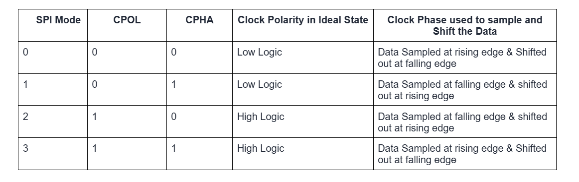
Figure 2 through Figure 5 show an example of communication in four SPI modes.
Multi-Sub-node Configuration
Multiple sub-nodes can be used with a single SPI main. The sub-nodes can be connected in regular mode or daisy-chain mode.
메타데이터
- post_id
- 2a78693fe1f3
- slug
- spi-serial-peripheral-interface-2a78693fe1f3
- url
- https://medium.com/@saintikumar3/spi-serial-peripheral-interface-2a78693fe1f3
- canonical_url
- https://medium.com/@saintikumar3/spi-serial-peripheral-interface-2a78693fe1f3
- author_url
- https://medium.com/@saintikumar3
- status
- ok
- fetched_at
- 2026-08-01 12:11:00