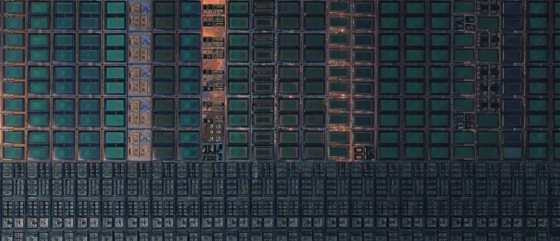
THE BRIGHT FUTURE OF VLSI : POWERED BY PHOTONICS
INTRODUCTION
THE BRIGHT FUTURE OF VLSI : POWERED BY PHOTONICS
INTRODUCTION
What is VLSI?
Very Large Scale Integration (VLSI) is the process of integrating thousands, millions or even billions of transistors(most commonly, MOS) on a single silicon-based chip.
Silicon became the dominant material to be used in this industry because of its electrical conductivity, thermal stability, natural formation of SiO2 layer, abundance in nature, crystalline structure that allows precise fabrication of ICs and supports miniaturization(Moore’s Law).
In VLSI design, every decision is guided by the PPA Matrix: Power — Since millions and billions of transistors are packed together, power efficiency is critical to avoid overheating and to extend battery life.
Performance — With the high density of components, speed and throughput define the usefulness of the chip.
Area — Minimizing the chip area while maximizing its functionality is the heart of the technology.
Limitations of Purely Electronic VLSI
A few of the concerning limitations are as follows:
· Electrical interconnects have resistance that reduces the speed of the signal. As the resistance is directly proportional to the length of the interconnect, electrical signals slow down over long distances.
· Signal delay and crosstalk increases as interconnect shrinks.
· Resistive loses in Copper interconnects generate heat. Also, cooling becomes a great matter of concern in highly dense chip.
· Leakage current reduces reliability.
· Shrinking wires and transistors to miniaturize the area of the chip further results in the increase in fabrication cost and defect rates.
2. CORE CONCEPTS
What is photonics enabled VLSI?
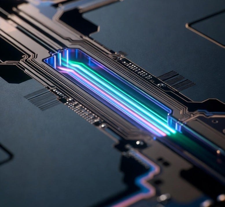
Photonics-enabled VLSI is the combination of photonic components with the traditional electronic VLSI components to overcome the limitations of purely electrical interconnects.
Methods
The core Methods in Photonics — enabled VLSI are:
· Silicon Photonics Integration: Fabrication of optical waveguides, modulators and waveguides directly onto the chip. This results in compact design and lower manufacturing cost.
· Optical interconnects: This method involves the replacement of electrical wires with optical links inside and between chips. Optical links(Example: waveguides) are pathways that use light to transfer data, instead of electrons. This method results in high bandwidth, low latency and reduced power consumption.
· Nano/micro photonic structures: This method uses micro‑ and nano‑scale optical wires, resonators, and gratings for routing and filtering signals. This enables compact, scalable photonic circuits.
· Hybrid electronic — photonic design: In this method, electronics handle the logic and control, whereas, data transfer is handled by photonics. This method balances the strength of both the domains.
· Wavelength Division Multiplexing (WDM): This method involves the sending of multiple optical signals at different wavelengths through the same waveguide. This dramatically increases the density of bandwidth without the need for additional physical interconnects.
· Optical packaging and Coupling: Optical packaging refers to the mechanical and material techniques used to protect and integrate photonic components such as waveguides, lasers, detectors into a chip or module. This ensures alignment, stability, and durability of optical devices. Optical coupling refers to the transfer of light between different parts of the system. This enables efficient chip — to — chip communication.
Approaches
· Monolithic integration: Fabrication of both electronic and photonic devices on the same Silicon chip. This approach exhibits high performance, but the process of fabrication is complex.
· Hybrid integration: To achieve better overall performance, this approach combines different materials on the same chip so that each material handles the function it is best at. Silicon is used for things like waveguides (to guide light) because it is easy to manufacture and works well with existing chip processes. Other materials such as Indium Phosphide or Germanium are added for tasks that Silicon is not good at, like generating light (lasers) or detecting light (photodetectors).
· Heterogeneous integration: This approach is about combining different chips made with different technologies into one package, so as to get the benefits of each without forcing them into a single manufacturing process. The electronics and photonic components are put together in a single package or system, instead of fabricating all the components on a single substrate. It uses advanced packaging such as 2.5D integration or 3D stacking.
· Optical Interconnect Approach: This approach replaces the traditional electrical wires with optical waveguides for the communication within and between the chips. This approach is often combined with WDM for massive bandwidth.
· Optical Network-on-Chip: In this approach, instead of electrical signals, optical signals are used to connect different modules inside a chip. This provides very high bandwidth, low latency, and energy-efficient communication.
· Co-Packaged Optics (CPO): It is an approach in photonics-enabled VLSI means putting optical communication parts directly inside the same package as the processor chip, so data moves faster and more efficiently than with traditional electrical connections.
Core Components
· Light sources: These devices produce optical signals and provide the initial light needed for the communication. Example: Lasers, LEDs
· Optical Modulators: These convert electrical signals to optical signals by changing the properties of light — intensity, phase, wavelength. Example: Mach-Zehnder modulators.
· Waveguides: They are path that guides light in the chip. They are usually made of Silicon because they are CMOS-compatible.
· Photodetectors: These convert optical signals back to electrical signals. Commonly used materials in the manufacturing of waveguides are Germanium and Indium Phosphide.
· Optical switches and routers: They control and direct the light signals along the chip. Used in Optical Network-on-Chip approach.
· Multiplexers and Demultiplexers: These allow multiple wavelengths of light to travel in the same waveguide. Multiplexers combine signals, demultiplexers separate them.
· Electronic control circuits: Electronic control circuits are the support system that makes photonic devices work properly inside a chip. They send electrical signals to drive modulators, stabilize lasers, amplify detector outputs, and keep everything synchronized with the digital logic. This circuit consists of driver circuits, bias circuits, amplifiers, clock and synchronization circuits, feedback and control loops, and signal conditioning circuits.
How it overcame the limitations of traditional VLSI?
Optical waveguides carry signals with almost zero resistance and hence speed is maintained even for longer distances.
Multiple optical signals can travel in the same waveguide using wavelength-division multiplexing (WDM), with minimal crosstalk compared to electrical wires. Delay is reduced because light avoids resistive-capacitive effects. Optical transmission has much lower energy loss, so less heat is generated. This reduces cooling requirements in dense chips.
Optical devices don’t suffer from leakage current like transistors. Reliability improves because signals are carried as photons, not electrons. Photonic interconnects allow scaling bandwidth without shrinking wires further. Instead of reducing the geometries of Copper, use of optical paths can reduce defect rates and ease fabrication challenges.
Difference between Photonics — enabled VLSI and Photonic ICs
Though Photonics-enabled VLSI and Photonics Integrated Circuits sound similar, they are distinct.
A few of their key differences are mentioned below:

3. PROS AND CONS
The pros and cons of the photonics-enabled VLSI are mentioned below:
Pros:
Optical interconnects can carry far more data than copper wires, supporting multi-terabit communication. Light signals avoid resistive-capacitive delays, enabling faster communication across the chip.
Less power is consumed per bit compared to electrical interconnects, reducing overall chip power usage. Optical transmission generates minimal heat compared to resistive losses in copper.
Supports communication among hundreds or thousands of cores, making it suitable for future many-core processors. Wavelength-division multiplexing (WDM) allows multiple signals to travel simultaneously in the same waveguide.
Cons: Integrating photonic devices with CMOS electronics requires advanced manufacturing techniques. Optical components sensitive to temperature changes, which can affect performance.
Aligning optical and electronic components precisely in hybrid or heterogeneous integration is difficult. Photonic integration is more expensive than traditional electronic VLSI due to specialized materials and processes.
Electronic design automation (EDA) tools are mature, but photonic design tools are still evolving. Long-term stability of photonic devices in dense chip environments is still under research.
4. CAREER PATHWAYS
JOB ROLES
PhD/Postdoc researcher: Work on cutting-edge topics like Optical Network-on-Chip (ONoC), co-packaged optics, or silicon photonics.
University faculty: Teaching and leading labs in photonics, VLSI design, or semiconductor technology.
Research scientist: Positions in institutes (MIT, IMEC, IITs, IISc, etc.) focusing on photonic integration and chip design.
Photonics IC Design Engineer: Design optical components (waveguides, modulators, detectors) integrated with CMOS.
VLSI/ASIC Engineer with photonics focus: Work on integrating photonic interconnects into large-scale chips.
Packaging and integration engineer: Specialize in co-packaged optics, heterogeneous integration, and advanced packaging.
Optical communication engineer: Develop systems that use photonics-enabled VLSI for high-speed data transfer.
EDA Tool developer: Create design tools for photonic circuits and hybrid VLSI-photonics systems.
CAREER AREAS:
AI hardware Architectures: Using photonics-enabled VLSI for faster neural network training.
Quantum photonics: Applying photonic VLSI concepts to quantum computing hardware.
Data Centre Infrastructure: Co-packaged optics and optical interconnects for next-gen cloud systems.
Startups & Entrepreneurship: Building companies around silicon photonics, optical interconnects, or chiplet-based architectures.
SKILLS AND TOOLS TO MASTER
Electronic Design Automation Tool :
Cadence Virtuoso, Synopsys, Mentor Graphics (Siemens EDA): for CMOS/VLSI design.
Lumerical, OptiFDTD, COMSOL Multiphysics: for photonic device simulation (waveguides, modulators, detectors).
Ansys HFSS: for electromagnetic simulations.
Layout and Verification tools:
KLayout, Magic VLSI: open-source tools for chip layout.
DRC/LVS tools: for design rule checking and verification.
Packaging and integration tools:
ANSYS Mechanical, Zemax OpticStudio: for optical packaging and alignment studies.
Hardware Description Language:
Verilog, VHDL, SystemVerilog: for digital circuit design and verification.
General purpose languages:
Python: widely used for automation, simulation scripting, and data analysis.
MATLAB: for modelling optical/electronic systems and signal processing.
C/C++: for performance-critical simulations and hardware-software co-design.
Specialized languages:
TCL: for scripting in EDA tools.
SPICE: for analog circuit simulation.
5. CONCLUSION
By harnessing light instead of electrons, the photonics enabled VLSI offers solutions to the limitations of the traditional VLSI, thereby increasing the overall performance of the chip. As computing demands continue to grow, photonics-enabled VLSI is poised to become a cornerstone technology, shaping the next generation of chips and redefining how we think about speed, scalability, and efficiency in modern electronics.
메타데이터
- post_id
- 2c27fe0305dd
- slug
- the-bright-future-of-vlsi-powered-by-photonics-2c27fe0305dd
- url
- https://medium.com/@rycenevlsitech/the-bright-future-of-vlsi-powered-by-photonics-2c27fe0305dd
- canonical_url
- https://medium.com/@rycenevlsitech/the-bright-future-of-vlsi-powered-by-photonics-2c27fe0305dd
- author_url
- https://medium.com/@rycenevlsitech
- status
- ok
- fetched_at
- 2026-06-21 22:26:41