FPGA DDR4 Read and Write Experiment
Performing a DDR4 read/write experiment on an FPGA can be quite involved, as it requires configuring both the FPGA and the DDR4 memory…
FPGA DDR4 Read and Write Experiment
Performing a DDR4 read/write experiment on an FPGA can be quite involved, as it requires configuring both the FPGA and the DDR4 memory interface correctly. Below is a guide that outlines how to perform a basic DDR4 read/write experiment on an FPGA, using an appropriate memory controller IP and the necessary tools.
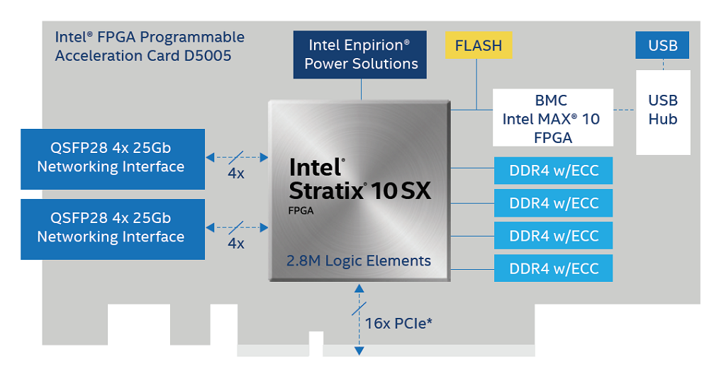
Overview of the Experiment
The basic idea of the experiment is to:
- Set up the DDR4 interface on the FPGA.
- Write data to the DDR4 memory.
- Read the data back from the DDR4 memory.
- Verify that the data read from DDR4 matches what was written.
This requires:
- A compatible FPGA development board (e.g., Intel/Altera FPGA board with DDR4 support).
- The DDR4 memory controller IP (provided by Intel or through third-party IP vendors).
- Quartus Prime or similar development tools.
Step-by-Step Guide
1. Set Up Your Development Environment
- Install Intel Quartus Prime: This is your main tool for designing with Intel FPGAs (previously Altera).
- Download or Locate DDR4 Memory Controller IP: Most FPGA boards with DDR4 support will have pre-designed DDR4 memory controller IP cores available. Intel’s Memory IP for DDR4 is available in the IP Catalog in Quartus Prime.
2. Create a New Project in Quartus
- Open Quartus Prime and create a new project.
- Select your FPGA device (e.g., Intel Cyclone V, Stratix 10, or Arria 10) from the available list.
- Define the directory and name for your project.
- Enable DDR4 interface (you can either use an existing board’s settings or manually configure the memory interface in your project).
3. Configure DDR4 Memory Interface
- Add DDR4 Memory Controller IP: In the Quartus project, go to Tools > IP Catalog, and search for the DDR4 controller IP. Use the configuration wizard to generate the controller based on the specifications of your memory chip (e.g., frequency, bus width, burst length).
- Example: For an Intel FPGA, this would typically be the DDR4 SDRAM Controller IP.
- Configure the controller for the correct clock, data width (usually 16 or 32 bits), and the memory’s timing parameters (e.g., CAS latency, number of memory banks, etc.).
- Pin Assignment: After generating the controller, assign the pins for DDR4 signals (CLK, CS, RAS, CAS, WE, etc.) in the Pin Planner. These pins are specific to your FPGA and the DDR4 DIMM.
4. Add a Simple Read/Write Testbench
To perform a DDR4 read/write experiment, you will need to create a simple testbench that sends read and write commands to the DDR4 controller.
Example of a basic VHDL/Verilog testbench:
- Write Operation:
- Write a known value to a specific memory address (e.g.,
0x0000). - Wait for the write operation to complete.
- Read Operation:
- Read back the data from the same memory address.
- Compare the read value with the written value.
Below is a simplified Verilog testbench example:
verilog

module ddr4_test;

reg clk;  // Clock signal
reg rst;  // Reset signal
reg [31:0] data_in;  // Data to write
wire [31:0] data_out;  // Data read from DDR4
reg [31:0] address;  // Address to read/write
reg write_enable;  // Control write enable
// Instantiate the DDR4 controller (generated IP)
ddr4_controller ddr4_inst (
    .clk(clk),
    .rst(rst),
    .address(address),
    .data_in(data_in),
    .data_out(data_out),
    .write_enable(write_enable)
);
// Clock generation
always begin
    #5 clk = ~clk;  // 100 MHz clock
end
initial begin
    // Initialize signals
    clk = 0;
    rst = 1;
    write_enable = 0;
    address = 32'h0000;  // Starting address for test
    data_in = 32'h12345678;  // Data to write
    // Reset the system
    #10 rst = 0;
    // Write data to DDR4
    #10 write_enable = 1;
    #10 write_enable = 0;  // Disable write after 1 clock cycle
    // Read back the data
    #10 address = 32'h0000;  // Read from the same address
    #10;  // Wait for the data to be read
    // Compare the read data with written data
    if (data_out == data_in) begin
        $display("Test Passed: Data read from DDR4 matches written data.");
    end else begin
        $display("Test Failed: Data read from DDR4 does not match written data.");
    end
    $finish;
end
endmodule
In this testbench:
- The write_enable signal controls when to write data into DDR4.
- After writing, the address is switched to read from the same location, and we verify if the data read matches what was written.
5. Compile the Design
- Compile the entire design in Quartus Prime. This step will synthesize the design, place-and-route the logic, and generate the bitstream (.sof file) for your FPGA.
6. Program the FPGA
- Connect your FPGA board to the computer via a USB-Blaster (or another programmer).
- In Quartus Prime, go to Tools > Programmer, select your FPGA hardware, and load the compiled bitstream (.sof) file.
- Program the FPGA.
7. Run the Test on the FPGA
- Once the FPGA is programmed, the testbench (in simulation or on the FPGA hardware) will run, performing the write and read operations on DDR4.
- If the read-back data matches the written data, your experiment is successful.
8. Debugging and Monitoring
- You can use the SignalTap II Logic Analyzer in Quartus to monitor signals on the FPGA in real-time and ensure that the DDR4 operations are functioning as expected.
- If any errors occur, use the Quartus console and waveform viewers to debug.
Conclusion
Performing a DDR4 read/write experiment on an FPGA involves:
- Setting up the DDR4 memory interface using the appropriate controller IP.
- Writing a simple read/write testbench to interact with DDR4.
- Compiling, programming, and verifying the experiment on the FPGA hardware.
This process requires good familiarity with FPGA design tools like Quartus, hardware description languages (HDL), and the memory controller IP.
메타데이터
- post_id
- 3e4cc2bd2ee1
- slug
- fpga-ddr4-read-and-write-experiment-3e4cc2bd2ee1
- url
- https://medium.com/@pqshedy33/fpga-ddr4-read-and-write-experiment-3e4cc2bd2ee1
- canonical_url
- https://medium.com/@pqshedy33/fpga-ddr4-read-and-write-experiment-3e4cc2bd2ee1
- author_url
- https://medium.com/@pqshedy33
- status
- ok
- fetched_at
- 2026-07-21 05:35:08