6-Layer PCBs Just Got an Upgrade: Is It Time to Switch to Via-in-Pad?
As hardware gets smaller and faster, our traditional layout tricks start to push their limits. If you regularly work on dense layouts, you…
6-Layer PCBs Just Got an Upgrade: Is It Time to Switch to Via-in-Pad?
As hardware gets smaller and faster, our traditional layout tricks start to push their limits. If you regularly work on dense layouts, you know that managing space on a multi-layer board feels like a game of high-stakes Tetris.
6-Layer PCBs Just Got an Upgrade: Is It Time to Switch to Via-in-Pad?
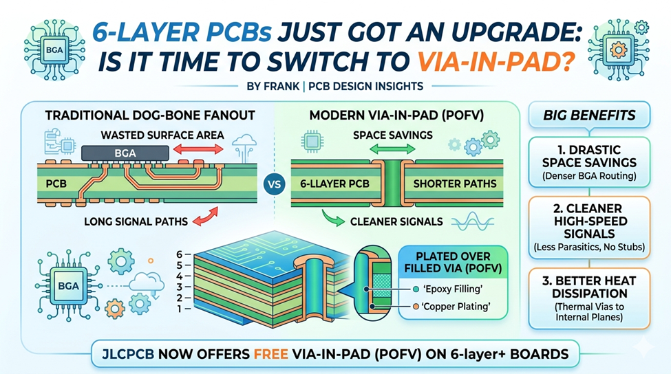
For years, senior engineers used traditional dog-bone fanouts to route signals away from fine-pitch components like Ball Grid Arrays (BGAs). But when you work with tight spacing, those little dog-bone traces eat up valuable surface space and choke your routing paths.
This is exactly why 6-layer boards are the sweet spot for many modern designs. They give you dedicated internal power and ground planes to control noise, while leaving the outer layers open for components. But today, the real upgrade for 6-layer layouts is Via-in-Pad technology.
What is Via-in-Pad, and Why Does it Matter?
In a traditional layout, you place your via outside the component pad and connect them with a short trace. Via-in-Pad changes this completely by putting the via hole directly inside the copper pad of your surface-mount component.
When you use this method, you instantly eliminate the fanout trace. This single change frees up an incredible amount of board real estate. If you want a deep dive into the physical structure of these holes, you can read more about what is a PCB via to understand how different types connect your layers.
Placing a standard open via inside a pad used to cause terrible assembly issues. During reflow soldering, the liquid solder would wick right down into the open hole like a straw. This left too little solder on the surface, creating weak joints or completely open circuits.
To solve this, manufacturers use a process called Plated Over Filled Via (POFV). They drill the via, fill the hole completely with a specialized epoxy paste, cure it with heat, flatten the surface, and then plate copper directly over the top. This creates a perfectly flat, solid copper pad that is fully solderable.
The Big Benefits
If you are on the fence about moving away from traditional fanouts, three major technical upgrades make Via-in-Pad worth the switch:
· Drastic Space Savings: By placing vias directly under BGA balls, you can escape signals from inner rows without using up surface routing channels. A tight 0.5 mm pitch BGA that usually requires eight layers might now fit easily on a 6-layer board.
· Cleaner High-Speed Signals: Shorter signal paths mean less parasitic inductance and capacitance. For high-speed lines, removing the fanout stub gets rid of impedance drops that cause signal reflections. You can learn more about managing these signals by checking out this guide to PCB via design best practices.
· Better Heat Dissipation: Filled vias acting as thermal pads create a direct solid copper highway to internal ground or power planes. This carries heat away from hot power ICs much faster than a thin surface trace ever could.
Is It Time to Make the Switch?
In the past, the choice to use Via-in-Pad came down to a painful budget decision. Because POFV requires extra drilling, epoxy filling, baking, and secondary copper plating steps, manufacturers always treated it as a premium feature. It added significant costs to prototyping and small production runs.
However, the manufacturing landscape has changed. To support hardware innovation, JLCPCB now offers free Via-in-Pad (POFV) as a default standard option for all 6-layer to 20-layer boards. They completely removed the price barrier for this advanced process, meaning you no longer have to pay a premium to use high-density routing techniques on your multilayer prototypes.
If your 6-layer design features fine-pitch components, high-speed lines, or tight spatial constraints, there is no longer a financial reason to stick to old dog-bone constraints. Designing with Via-in-Pad gives you cleaner routing, stronger signal integrity, and cooler components without hurting your project budget.
I highly recommend watching this practical video demonstrating how these advanced multi-layer capabilities change the layout workflow:
Advanced 6-Layer PCBs and Via-in-Pad Features
This video walks through the exact fabrication quality and layer structures of modern 6-layer boards using filled-and-capped via technology.
메타데이터
- post_id
- 3ecfc2034164
- slug
- 6-layer-pcbs-just-got-an-upgrade-is-it-time-to-switch-to-via-in-pad-3ecfc2034164
- url
- https://medium.com/@frankblog25/6-layer-pcbs-just-got-an-upgrade-is-it-time-to-switch-to-via-in-pad-3ecfc2034164
- canonical_url
- https://medium.com/@frankblog25/6-layer-pcbs-just-got-an-upgrade-is-it-time-to-switch-to-via-in-pad-3ecfc2034164
- author_url
- https://medium.com/@frankblog25
- status
- ok
- fetched_at
- 2026-06-09 15:37:30