Fractal Geometry Semiconductors Processing: The Plasma Role
The technical review paper cited here examines the semiconductor industry’s response to the approaching physical and economic limits of…
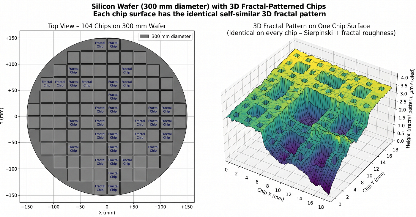
Figure 1: Multi-scale visualization of fractal surface integration. Left: 300 mm silicon wafer layout featuring 104 individual chips. Right: 3D isometric view of an 18.0 mm × 18.0 mm chip surface showing hierarchical topography — combining a recursive Sierpinski carpet pattern with fractal roughness.
Fractal Geometry Semiconductors Processing: The Plasma Role
The technical review paper cited here examines the semiconductor industry’s response to the approaching physical and economic limits of Moore’s Law. The paper traces the evolution of computing architectures from thermionic vacuum tubes through modern heterogeneous systems, demonstrating how advanced physical plasma etching technologies and non-Euclidean design principles enable continued computational scaling beyond traditional lithographic miniaturization [1].
Historical Context
The paper establishes that electronic computing has progressed through distinct paradigms, beginning with thermionic gaseous electronics (vacuum tubes) and transitioning to solid-state semiconductors. A parallel manufacturing revolution shifted from isotropic wet chemical etching — which produced undercutting and limited precision — to anisotropic dry physical plasma etching (Reactive Ion Etching (RIE) and Atomic Layer Etching (ALE)), enabling sub-nanometer precision and high-aspect-ratio structures essential for modern chip design.
The End of Classical Moore’s Law
The industry now faces binding constraints that prevent continued transistor density growth through traditional miniaturization alone:
- Power Wall: Quantum tunneling effects at sub-2 nm nodes cause unsustainable leakage and thermal density.
- Economic Wall: Extreme ultraviolet lithography and advanced packaging have become prohibitively expensive.
- Reticle Limits: Photolithography cannot economically produce dies larger than ~800 mm².
The “More than Moore” Paradigm Shift
Rather than pure geometric shrinking, the industry is adopting heterogeneous integration and topological complexity:
- Intel Xeon 6: Disaggregates into 12 small compute tiles connected via Embedded Multi-Die Interconnect Bridge (EMIB), with TDP capped at 300–500W.
- NVIDIA GB200: Integrates one Grace CPU and two Blackwell GPUs using Chip-on-Wafer-on-Substrate packaging with mandatory liquid cooling (1200–2700W), achieving ~20 PFLOPS in AI-optimized precisions.

Figure 2. Transistor count (log scale) for 24 landmark processors from the Intel 4004 (1971) to projected fractal-era chips (2032), colour-coded by era: planar Moore’s Law adherence (blue), Power Wall–driven slowdown at sub-2 nm nodes (amber), heterogeneous chiplet pivot via Intel EMIB and NVIDIA CoWoS (purple), and post-lithographic recovery through Sierpinski-pattern fractal geometries with PE-ALE (+21% surface area, green). The grey dashed line denotes the ideal classical trajectory (2× per two years); divergence after 2020 marks the transition from dimensional miniaturisation to topological scaling.
Fractal Geometries as a Solution
The paper proposes non-Euclidean fractal architectures (e.g., Sierpinski carpet patterns combined with stochastic roughness) as a pathway to increase effective transistor density without further shrinking. A quantitative comparison shows that 3D fractal chips can achieve approximately 21% more usable surface area on identical physical footprints, potentially extending Moore’s Law through topological expansion. Higher recursion levels could yield 2–5× multiplication factors.
Enabling Technology: Advanced Plasma Etching
Modern plasma technologies are indispensable for realizing these complex architectures:
- RIE/ICP-RIE: Delivers angstrom-to-nanometer precision for 3D stacking, FinFETs, and chiplet interconnects
- Atomic Layer Etching (ALE): Provides atomic-scale control, exceptional selectivity (>100:1), and minimal damage — essential for Gate-All-Around transistors and fractal topologies
Conclusion
The semiconductor industry is not reaching saturation but transitioning from miniaturization-driven growth to a synergy of advanced plasma physics, fractal mathematics, and heterogeneous system integration. By combining atomic-layer precision with 3D topological expansion, manufacturers can sustain more computational growth into the 21st century. The shape of the chip itself becomes as important as the transistors it contains, marking a reintroduction of complexity in post-lithographic semiconductor design.
— — —
[1] Ahmed M. Hala “Fractal Geometry Computing Architectures: Review of Plasma-Enabled Scaling and the Transition to non-Euclidean Shaped Semiconductor Chips Design” (2026) https://doi.org/10.5281/zenodo.19827158
메타데이터
- post_id
- 42eca808977a
- slug
- fractal-geometry-semiconductors-processing-the-plasma-role-42eca808977a
- url
- https://medium.com/@amhala/fractal-geometry-semiconductors-processing-the-plasma-role-42eca808977a
- canonical_url
- https://medium.com/@amhala/fractal-geometry-semiconductors-processing-the-plasma-role-42eca808977a
- author_url
- https://medium.com/@amhala
- status
- ok
- fetched_at
- 2026-06-10 18:44:10