How to Reduce PCB Stress in High-Density Assemblies
In modern electronics manufacturing, PCB stress is becoming one of the more critical — but often underestimated — factors affecting product…
How to Reduce PCB Stress in High-Density Assemblies
In modern electronics manufacturing, PCB stress is becoming one of the more critical — but often underestimated — factors affecting product reliability.
As PCB designs continue to evolve in 2026, manufacturers are working with:
- Smaller board sizes
- Higher component density
- More sensitive electronic structures
- Tighter spacing between components and board edges
These changes improve product performance and compactness, but they also reduce the mechanical tolerance of the assembly process.
As a result, even small amounts of mechanical stress during manufacturing can lead to long-term reliability issues.

Why PCB Stress Matters More in High-Density Designs
In high-density PCBA, components are often placed very close to:
- Board edges
- Routing paths
- Depaneling lines
This makes them more vulnerable to mechanical forces introduced during production steps such as handling, fixture clamping, and depaneling.
Excessive stress may lead to:
⚠️ Micro-cracks in solder joints ⚠️ Component lift or misalignment ⚠️ Latent reliability failures ⚠️ Reduced product lifespan
One of the most challenging aspects is that these issues are not always immediately visible during inspection.
In many cases, boards may pass initial quality checks but fail later during:
- Thermal cycling
- Functional testing
- Field operation
This is why stress control is increasingly being treated as a system-level manufacturing concern rather than a single-process issue.
Where PCB Stress Commonly Occurs
PCB stress can be introduced at multiple stages of manufacturing. The most critical areas include:
1. PCB Handling and Fixturing
Improper handling or uneven fixture support can introduce bending or localized pressure on the board.
This is especially important for thin or flexible substrates, where structural rigidity is limited.
2. SMT Assembly Process
Although SMT is highly automated, mechanical stress can still occur during:
- Board transport
- Clamping in equipment
- Reflow carrier handling
These forces may not always be obvious, but can accumulate over time.
3. Depaneling Process
One of the most significant sources of mechanical stress is PCB depaneling.
Depending on the method used, depaneling can introduce:
- Vibration
- Cutting force
- Mechanical shock
- Edge stress concentration
This is particularly critical for high-density assemblies where sensitive components are located near separation lines.
Low-Stress Depaneling Methods
To reduce mechanical impact, many manufacturers are now adopting low-stress depaneling strategies.
Precision Router Depaneling
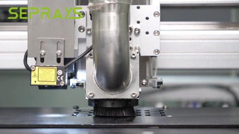
Router systems use controlled mechanical cutting tools to separate PCBs.
Key advantages:
- Flexible cutting paths
- Good control over the cutting process
- Suitable for complex PCB outlines
When properly optimized, router systems can help reduce uncontrolled stress compared to manual or less controlled methods.
Laser Depaneling
Laser-based systems eliminate physical contact during cutting.
Key benefits include:
- Minimal mechanical stress
- High precision cutting capability
- Suitable for sensitive and high-density PCBA
This method is increasingly used in applications where reliability is critical, such as:
- Medical electronics
- Semiconductor-related devices
- High-reliability industrial systems
Fixture and Process Optimization
Beyond the cutting method itself, fixture design plays a crucial role in stress reduction.
Proper support systems can:
- Prevent PCB bending
- Stabilize cutting paths
- Reduce vibration during processing
In many cases, fixture optimization is as important as equipment selection.
Industry Trend in 2026
One noticeable shift in electronics manufacturing is how PCB depaneling is being viewed.
Traditionally, it was considered a final mechanical step in production.
Now, it is increasingly seen as part of the overall:
- Yield optimization strategy
- Reliability control system
- Quality assurance process
Manufacturers are no longer focusing only on: 👉 speed and throughput
Instead, more attention is being given to: ✔ process stability ✔ stress reduction ✔ hidden defect prevention ✔ long-term product reliability
Why This Matters
As electronic devices become more compact and performance-driven, small manufacturing variations can have amplified effects on final product behavior.
Reducing PCB stress is not just about improving immediate yield — it is also about ensuring long-term stability and performance in real-world applications.
Final Thoughts
There is no single solution that fits every PCB design or production environment.
The best approach depends on:
- Board structure
- Component sensitivity
- Production volume
- Reliability requirements
- Manufacturing constraints
However, one thing is clear:
As high-density assemblies continue to evolve, controlling PCB stress will remain a key factor in maintaining consistent quality and long-term reliability.
For a more detailed discussion, you can refer to the original article here: https://seprays.com/how-to-reduce-pcb-stress-in-high-density-assemblies/
메타데이터
- post_id
- 5c645be2ea5c
- slug
- how-to-reduce-pcb-stress-in-high-density-assemblies-5c645be2ea5c
- url
- https://medium.com/@sales_40837/how-to-reduce-pcb-stress-in-high-density-assemblies-5c645be2ea5c
- canonical_url
- https://medium.com/@sales_40837/how-to-reduce-pcb-stress-in-high-density-assemblies-5c645be2ea5c
- author_url
- https://medium.com/@sales_40837
- status
- ok
- fetched_at
- 2026-06-13 12:55:53