Should We Opt for Single Layer or Double Layer Flex PCB?
In flexible electronics design, a single most influential choice engineers have to make is whether to opt for a single layer or double…
Should We Opt for Single Layer or Double Layer Flex PCB?
flex PCB
In flexible electronics design, a single most influential choice engineers have to make is whether to opt for a single layer or double layer flex PCB. This decision affects directly the circuit complexity, cost of the manufacturing, lead time and long-term reliability. Knowing the difference — including the process of manufacturing double layer flex PCBs — enables you to make a better, cost-efficient choice. Collaborating closely with an experienced flex PCB manufacturer from the early stage of design is highly advised.
What Is a Single Layer Flex PCB
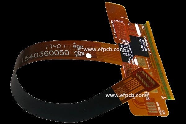
Single layer flex PCB has copper traces only on one side of the flex polyimide substrate. It is the most basic type of flexible circuit and contains a base film, a single layer of copper, and a coverlay for protection on the top. Since of its simple construction, single layer flex PCBs are light in weight, extremely flexible and feasible to produce. A good flex PCB maker can make them with relatively low tooling costs and in short lead times. They also find applications in LED lighting strips simplesensors connections, consumer electronics ribbon cables and medical wearable devices in which complexity of routing is not high. The process for making one layer boards is simple. It includes the preparation of laminate, photolithography patterning, copper etching, coverlay laminating, surface finishing, and electrical testing. Less processing steps would result in less defect possibility and faster turn around time.
What Is a Double Layer Flex PCB
A double layer flex PCB has copper traces on the both sides of the polyimide substrate and the two conductive layers are electrically connected through plated through holes. This severely enhances routing density and routing flexibility, allowing even more complex electronic assemblies. Any experienced flex PCB manufacturer will tell you double layer construction allows for possibilities you will not have in a single layer — including signal crossovers, differential pair routing, power and ground plane separation, and densier component integration.
Double Layer Flex PCB Manufacturing Process and Key Characteristics
Double layer flex PCBs are more complex to produce as they have additional layer and tighter tolerance then single layer boards. Below is a more detailed listing of the major production stages.
Material Selection and Laminate Preparation
The starting material is a double-sided copper-clad polyimide laminate, generally 12.5 µm to 50 µm thick. Polyimide is selected because of its superior thermal stability, chemical inertness and high mechanical flexibility. A reputable flex PCB manufacturer will select the laminate material suitable for the application of the bend radius, operating temperature, and signal frequency.
Drilling and Via Formation
Accurate drilling techniques are used to form the through holes, which connect the top and bottom copper layers. Laser drilling is employed to produce holes smaller than 100 µm in fine-pitch applications. Mechanical drilling is used for big vias. Hole placement needs to be precise — if the hole is off at this point, the entire board is electrically compromised.
Electroless Copper Deposition and Electroplating
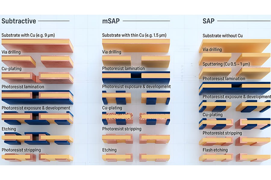
After drilling, the panel is subjected to electroless copper deposition to cover the hole walls with a layer of conductive seed. Then, the via walls are plated with electrolytic copper to achieve the desired thickness (typically in the 20 um to 25 um range). This plated through hole is the structure that provides double layer flex PCB’s inter-layer conduction. Experienced flex PCB manufacturers all watch plating uniformity very closely to maintain uniform electrical performance.
Photolithography and Copper Etching
A dry film photoresist is laminated on each side of the panel, exposed under UV light through the circuit artwork film, and chemically developed. The excess copper is then etched away, leaving the exact path patterns on both layers. A good flex PCB manufacturer should have tight registration between the top and bottom layers, and the manufacturer should use high-end optical alignment equipment to confine layer-to-layer accuracy of ±25 µm.
Coverlay Lamination
Flex PCBs do not have a soldermask similar to rigid PCBs, instead they have a polyimide coverlay film which is bonded with adhesive under the influence of heat and pressure. The “passivated” coverlay protects copper traces from oxidation, mechanical abrasion and exposure to the elements while maintaining the flexibility of the board. This lamination process needs to be carried out with exact temperature and pressure profiles. An expert flex PCB manufacturer will consider coverlay lamination as one of the critical operation in production.
Surface Finish Application
There is a surface finish applied to the exposed copper pads to help with the solderability and to prevent further oxidation. Popular choices are ENIG, immersion silver, immersion tin and OSP. ENIG is widely used in double layer flex PCB for its smooth surface, good solderability and compatibility with fine pitch components.
Routing, Electrical Testing and Inspection
The panel is routed using laser cutting or mechanical routing to singulate the board. Then each board is tested electrically with flying probe test, to check for continuity and isolation. High quality flex PCB manufacturer also conducts AOI and cross-section test on sample panels to prove the quality of via plating and trace integrity prior to shipment. Double layer flex PCBs are significantly more costly when it comes to drilling and plating and alignment processes. Nevertheless, the higher cost is fully justified when complexity of the circuit demands it. An experienced flex PCB manufacturer can assist you in determining if your design really requires two layers or if intelligent single layer routing can provide the same functionality for less cost.
How to Avoid Making a Bad Choice
The choice between single and double layer flex PCB is therefore determined by the complexity of the circuit, the size of the space and the cost. Use single layer for simple point-to-point connections, when routing space is abundant and you are with tight budget. Use double layer for signal crossovers, higher component density, and controlled impedance routing when these cannot be achieved on a single layer. Working with a reputable flex PCB manufacturer can help that happen right at the start of your design. An experienced flex PCB manufacturer will analyse your schematic based on your routing issues and propose the most cost effective construction. The best **flex PCB manufacturer** isn ’ t just a dispatcher for your order — they help you design a better, more manufacturable product from day one.
메타데이터
- post_id
- 5dfedb4dc6b7
- slug
- should-we-opt-for-single-layer-or-double-layer-flex-pcb-5dfedb4dc6b7
- url
- https://medium.com/@wyg28291/should-we-opt-for-single-layer-or-double-layer-flex-pcb-5dfedb4dc6b7
- canonical_url
- https://medium.com/@wyg28291/should-we-opt-for-single-layer-or-double-layer-flex-pcb-5dfedb4dc6b7
- author_url
- https://medium.com/@wyg28291
- status
- ok
- fetched_at
- 2026-07-11 06:06:52