Why PCB Technology Is Now the Center of the AI Hardware Race
If you’ve been following the AI hardware conversation, you’ve probably noticed something shifting. The discussion used to be about chips —…
Why PCB Technology Is Now the Center of the AI Hardware Race
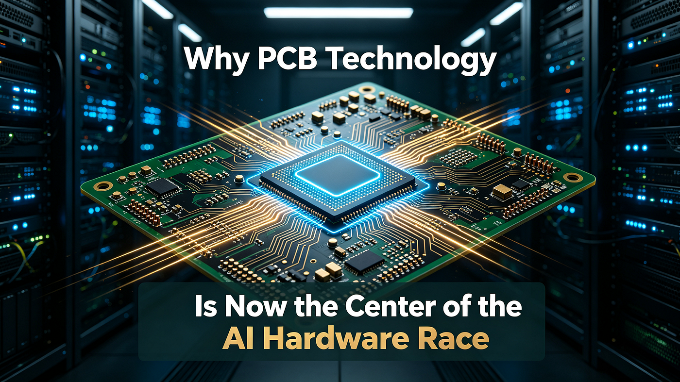
If you’ve been following the AI hardware conversation, you’ve probably noticed something shifting. The discussion used to be about chips — more GPUs, more FLOPS, more bandwidth. But in 2026, the conversation has moved to something less glamorous but equally critical: the circuit boards that hold it all together.
AI servers are pushing PCB technology to its absolute limits. And in doing so, they’ve turned circuit boards from a commodity into a strategic bottleneck.
The Numbers That Tell the Story
A standard server motherboard uses 8–16 layers of FR-4 material. An AI server? 16–24 layers minimum — with next-generation designs pushing toward 28–32 layers. The difference isn’t just about layer count; it’s about everything else.

The cost difference isn’t just about materials. It’s about capability. AI server boards require mSAP (Modified Semi-Additive Process) — which starts with an ultra-thin copper seed layer and electroplates traces instead of etching them from full copper foil. This eliminates etch undercut and enables trace widths down to 30μm in production.
The Manufacturing Reality: What Actually Changed
1. Copper Foil: HVLP4 Is Now the Baseline
At 56 GHz and above, the electromagnetic skin depth in copper is only 0.3–0.4μm. Standard copper foil with surface roughness of 8–12μm forces current to travel a longer effective path, increasing resistive loss.
HVLP4 (Hyper Very Low Profile) foil reduces surface roughness from 4μm to below 2μm, recovering 2–3 dB of insertion loss across a 6-inch backplane trace. That 2.5 dB margin can mean the difference between a compliant 112G PAM4 channel and a failing one.
In 2025–2026, HVLP3 was the mainstream spec. By the end of 2026, HVLP4 is expected to become the standard for next-generation AI servers.
2. Copper Weight: Heavy Copper Is No Longer Optional
AI GPUs now consume 700–1000W each, with next-generation designs pushing toward 1500W. Delivering that power through the PCB requires heavy copper inner layers of 2–3oz, extensive via arrays for vertical power delivery, and careful power integrity design.
Some manufacturers are now supporting heavy copper up to 10oz (350μm) on both inner and outer layers, allowing the PCB to function as a heat spreader.
3. Back Drilling: Stubs Are “Zero Tolerance”
At 112G PAM4 speeds, even 8–10mil of residual via stub creates resonance frequencies that fall within the signal bandwidth. Back drilling removes the unused via barrel to improve signal integrity.
4. Materials: Ultra-Low-Loss Laminates Are Now Standard
Standard FR-4 has a Df (dissipation factor) of about 0.02. AI server PCBs require materials like Panasonic Megtron 6 (Df 0.002), Isola Astra MT77 (Df 0.0017), or Megtron 7 for the most demanding channels.
The Cost of Getting It Right
A 24-layer ultra-HDI AI server board with mSAP processing can cost $80–200 per unit, compared to $15–25 for a standard 12-layer FR-4 board.
But the real cost is what happens if you get it wrong. Failed signal integrity means system-level failure. Marginal insertion loss means retimers and higher power consumption. Poor thermal design means accelerated component aging.
That’s why the industry is investing over $4 billion in cumulative PCB manufacturing capacity targeting ultra-HDI capabilities from 2025–2027.
The Bottom Line
The PCB is no longer just a passive carrier for components. In AI hardware, it’s an active part of the system design — and in many cases, it’s the bottleneck.
If you’re designing AI hardware in 2026, the board is not something you spec at the end of the project. It’s something you start with.
📬 We’re a PCBA manufacturer specializing in small-to-medium batches — from prototypes to production. If you’re designing AI hardware and need a partner who understands the technical demands, send us your files. We’ll provide a DFM review and a transparent quote.
메타데이터
- post_id
- 6a7f4ebb808a
- slug
- why-pcb-technology-is-now-the-center-of-the-ai-hardware-race-6a7f4ebb808a
- url
- https://medium.com/@AnyPCBA_Official/why-pcb-technology-is-now-the-center-of-the-ai-hardware-race-6a7f4ebb808a
- canonical_url
- https://medium.com/@AnyPCBA_Official/why-pcb-technology-is-now-the-center-of-the-ai-hardware-race-6a7f4ebb808a
- author_url
- https://medium.com/@AnyPCBA_Official
- status
- ok
- fetched_at
- 2026-08-19 21:23:57