SanDisk Moves Beyond HBF: Patent Shows Processor Bonded to NAND Flash With HBM Stacks on a Shared…
SanDisk is accelerating development of High Bandwidth Flash (HBF), a next-generation architecture that vertically stacks NAND, while also…
SanDisk Moves Beyond HBF: Patent Shows Processor Bonded to NAND Flash With HBM Stacks on a Shared Interposer
SanDisk Moves Beyond HBF
SanDisk is accelerating development of High Bandwidth Flash (HBF), a next-generation architecture that vertically stacks NAND, while also advancing other memory concepts aimed at overcoming structural capacity limits.
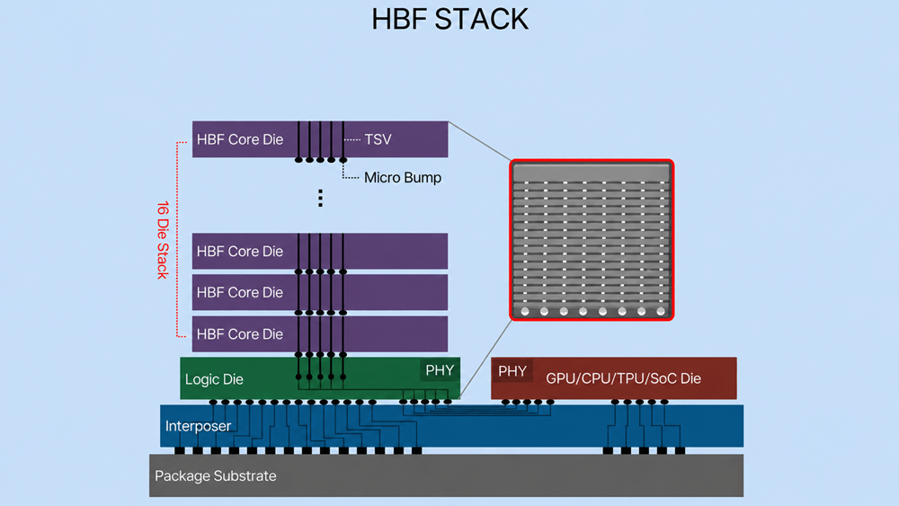
According to a previously filed and published U.S. patent from SanDisk, US 12,430,274 B2, the design integrates a multi-core processor directly onto a CBA (CMOS Bonded Array) memory unit. That memory unit itself combines a large NAND flash array with a CMOS logic layer.
SanDisk says the integrated stack is then mounted on an interposer, with HBM semiconductor chip stacks attached to one or more sides of the combined stack.
Design Rationale
As noted by Wccftech, the motivation behind SanDisk’s approach is tied in part to the inherent limitations of HBM, especially its relatively limited capacity, as well as unresolved challenges in HBF such as latency, power efficiency, and system-level integration complexity.
To address HBM’s capacity ceiling, SanDisk previously introduced the HBF architecture. Like HBM, it relies on vertically stacking multiple layers of NAND flash and connecting them through through-silicon vias (TSVs) to form a unified memory stack.
Current HBM solutions typically offer 32GB to 64GB per stack, while HBF is designed for far greater scalability, with reported capacities of up to 4TB. SanDisk says HBF can deliver 8 to 16 times the capacity of HBM at roughly comparable cost, while maintaining bandwidth close to HBM levels.
However, although NAND flash offers higher capacity and lower cost, it is also farther from the compute chip, which makes data access slower than DRAM-based architectures. To address this, SanDisk’s latest patent proposes a 3D stacked design in which a NAND flash chip built with the CBA structure sits beneath a compute chip such as an AI accelerator or GPU.
In this configuration, HBM DRAM remains integrated on the same interposer, but it serves a different role within the broader memory-compute hierarchy. According to the report, this allows HBM to handle immediate, high-speed memory operations, while the NAND flash layer within the memory unit is used for read/write-intensive workloads and large-scale data storage.
(Source: SanDisk)
메타데이터
- post_id
- 8cfb249e3922
- slug
- sandisk-moves-beyond-hbf-patent-shows-processor-bonded-to-nand-flash-with-hbm-stacks-on-a-shared-8cfb249e3922
- url
- https://medium.com/@avaq-ic/sandisk-moves-beyond-hbf-patent-shows-processor-bonded-to-nand-flash-with-hbm-stacks-on-a-shared-8cfb249e3922
- canonical_url
- https://medium.com/@avaq-ic/sandisk-moves-beyond-hbf-patent-shows-processor-bonded-to-nand-flash-with-hbm-stacks-on-a-shared-8cfb249e3922
- author_url
- https://medium.com/@avaq-ic
- status
- ok
- fetched_at
- 2026-07-20 02:51:28