PCB Board Fabrication: A Complete Guide to Process, Challenges & Best Practices
1. Overview: Why PCB Board Fabrication Matters
PCB Board Fabrication: A Complete Guide to Process, Challenges & Best Practices
1. Overview: Why PCB Board Fabrication Matters
In today’s hyper-connected world, virtually every piece of electronic equipment — from a smartphone in your pocket to a satellite orbiting the Earth — relies on one foundational component: the Printed Circuit Board (PCB). PCB board fabrication is the precise, multi-step manufacturing process that transforms a digital schematic into a physical, functional circuit board capable of carrying electrical signals across components with pinpoint accuracy.
This guide is designed for engineers, product developers, procurement professionals, and electronics enthusiasts who want a thorough understanding of what PCB board fabrication involves, how it works, and how to choose the right fabrication partner. Whether you are developing a PCB prototype for the first time or scaling an existing design into mass production, understanding the fabrication process empowers you to make smarter design decisions, reduce costly revisions, and accelerate your time to market.
PCB board fabrication is not simply a manufacturing task — it is a science-driven engineering process where every micrometer matters. A deviation in trace width, a misaligned layer, or an improperly drilled via can render an otherwise perfect design completely non-functional.
This article covers: what PCB board fabrication is, the step-by-step fabrication process (including its overlap with embedded system design), common fabrication defects and how to resolve them, frequently asked questions, and a look at how TJHX PCB delivers world-class custom fabrication services to global clients.
2. What Is PCB Board Fabrication?
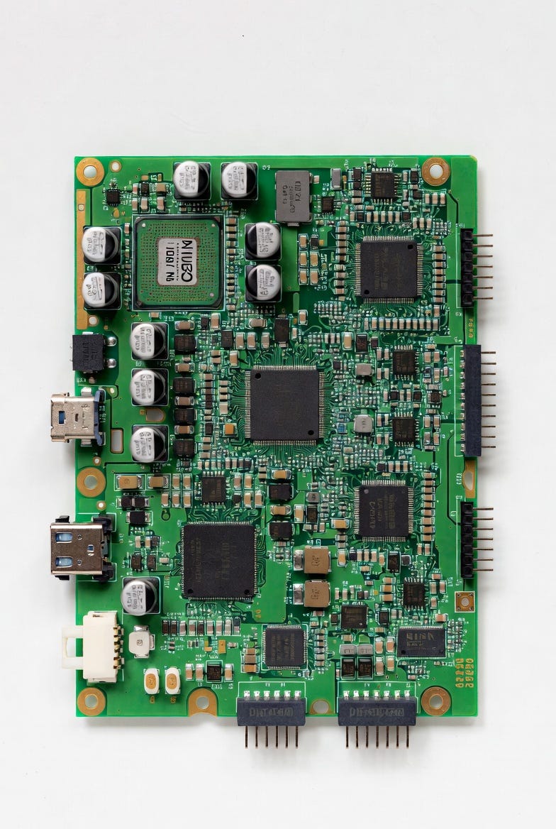
PCB board fabrication refers to the end-to-end process of creating a bare printed circuit board — that is, the physical board structure before any electronic components are mounted on it. It encompasses everything from design verification and material selection to imaging, etching, drilling, plating, solder mask application, surface finishing, and electrical testing.
A printed circuit board is a flat, rigid (or flexible) substrate — most commonly made from FR-4 fiberglass-reinforced epoxy laminate — that mechanically supports electronic components while electrically connecting them using conductive copper pathways known as traces, pads, and vias.
PCB board fabrication is distinct from PCB assembly (PCBA). Fabrication produces the bare board, while assembly involves soldering components (resistors, capacitors, ICs, connectors, etc.) onto the fabricated board. Together, these two processes form what is commonly referred to as the full PCB manufacturing workflow.
Key Types of PCBs Produced Through Fabrication
• Single-Layer PCB — Conductive copper on one side only; ideal for simple, low-cost applications such as calculators and LED lighting.
• Double-Layer PCB — Copper layers on both sides connected by plated through-holes (PTH); used in power supplies, amplifiers, and consumer electronics.
• Multi-Layer PCB — Four or more conductive layers laminated together; essential for complex applications such as servers, routers, and medical devices.
• Rigid PCB — Standard solid board construction using FR-4; the most common form factor.
• Flexible PCB (FPC) — Made from polyimide or similar materials; used in wearables, cameras, and space-constrained devices.
• Rigid-Flex PCB — A hybrid combining rigid and flexible sections; used in aerospace, military, and advanced medical equipment.
• HDI PCB (High-Density Interconnect) — Features micro-vias, fine traces, and high-density routing; critical for smartphones, tablets, and miniaturized electronics.
The choice of PCB type directly influences the fabrication process complexity, material requirements, lead time, and overall cost. Understanding these distinctions upfront is essential for any engineer or product manager involved in PCB board fabrication planning.
3. The Complete PCB Board Fabrication Process: Step-by-Step
PCB board fabrication is a meticulously controlled, sequential process. Each step builds upon the previous one, and any defect carried forward can compound into a serious functional failure. Below is a comprehensive breakdown of the fabrication workflow, which also forms the backbone of embedded system design when hardware is being realized from concept to prototype.

Step 1: Schematic Design & PCB Layout
The fabrication journey begins with the electronic design. Using EDA (Electronic Design Automation) software — such as Altium Designer, KiCad, OrCAD, or Eagle CAD — engineers create a schematic diagram that captures the logical relationships between all components. This schematic is then translated into a physical PCB layout, where component placement, routing of traces, and layer stack-up are defined.
For embedded system design in particular, this stage is critical. The PCB must accommodate a microcontroller or microprocessor, power regulation circuits, memory interfaces, communication buses (SPI, I2C, UART, USB, Ethernet), and sensor inputs — all while respecting signal integrity, impedance control, and EMC guidelines.
Step 2: Design Rule Check (DRC) & DFM Review
Before any file is submitted to the fabrication facility, the design undergoes a Design Rule Check (DRC) within the EDA software and a Design for Manufacturability (DFM) review by the manufacturer. DRC validates that traces meet minimum width requirements, clearances between conductors are sufficient, drill hole sizes are within tolerance, and no design violations exist.
DFM review goes a step further by checking whether the design is physically achievable with the manufacturer’s specific equipment and processes. Issues flagged here — such as annular ring violations, copper-to-edge clearances, or unsupported via-in-pad designs — are resolved before fabrication begins, saving enormous time and cost.
Step 3: Gerber File Generation & Engineering Order
Once the design is approved, the engineer exports Gerber files (typically in RS-274X or the newer Gerber X2 format), drill files (Excellon format), and a BOM (Bill of Materials). These files serve as the complete fabrication package, encoding every layer of the PCB including copper layers, solder mask layers, silkscreen layers, board outline, and drill data.
The PCB fabrication house processes these files to generate a manufacturing engineering order, defining the exact materials, processes, tolerances, and quality checks required for that specific design.
Step 4: Material Selection & Inner Layer Preparation
The substrate material is selected based on the application’s electrical, thermal, and mechanical requirements. FR-4 is the most widely used material. High-frequency applications may require Rogers or PTFE-based materials. For multilayer PCBs, inner copper layers are first prepared by laminating thin copper foil sheets onto pre-preg (pre-impregnated) fiberglass sheets.
The inner layer copper is then coated with a photosensitive dry film resist and exposed to UV light through a photomask derived from the Gerber files. The exposed areas harden, protecting the copper beneath, while the unexposed areas are chemically removed to reveal the unwanted copper for etching.
Step 5: Copper Etching
In the etching process, the board is immersed in a chemical etchant — typically alkaline ammonia or ferric chloride — which selectively removes the exposed copper that is not protected by the hardened photoresist. What remains after etching are the precise copper traces, pads, and planes defined by the PCB layout. This step demands tight control of etchant concentration, temperature, and immersion time to achieve accurate trace widths.
Step 6: Layer Alignment & Lamination (for Multi-Layer PCBs)
For multilayer PCB board fabrication, the individual inner layers are precisely aligned using optical inspection equipment and registration targets (fiducials). The layers — alternating between core materials and pre-preg sheets — are stacked, aligned, and bonded together under high heat and pressure in a hydraulic lamination press. This process creates a solid, monolithic board structure.
Step 7: Drilling
After lamination, the board is drilled using high-speed CNC drilling machines to create through-holes (for through-hole components and plated vias) and, in HDI boards, laser-drilled micro-vias (blind and buried vias). Drilling precision is critical — a misaligned hole can damage inner-layer copper and compromise electrical connectivity.
Step 8: Copper Plating (PTH & Electroplating)
The drilled holes are cleaned and then coated with a thin layer of electroless copper through a chemical deposition process, making the hole walls conductive. This is followed by electrolytic copper plating to build up the copper thickness to the required level (typically 25 microns for standard PTH), ensuring reliable electrical connections between layers.
Step 9: Outer Layer Imaging & Etching
Similar to the inner layer process, the outer layers are coated with photoresist, exposed through photomasks derived from the Gerber files, developed, and etched to form the final outer copper circuitry. A tin plating step is often applied beforehand to protect the copper traces during the outer etch process.
Step 10: Solder Mask Application
A liquid photoimageable (LPI) solder mask — typically green, though other colors such as black, blue, red, yellow, and white are available — is applied to both sides of the board. The solder mask protects copper traces from oxidation, prevents solder bridging during assembly, and provides electrical insulation. Only the pads that need to be soldered remain exposed.
Step 11: Silkscreen (Legend) Printing
A silkscreen layer is printed onto the solder mask surface using inkjet or screen printing, adding component reference designators, polarity markings, logos, revision numbers, and other human-readable information. This layer is essential for PCB assembly and field maintenance.
Step 12: Surface Finish Application
The exposed copper pads — not covered by solder mask — are treated with a surface finish to protect them from oxidation and enhance solderability. Common surface finishes include:
• HASL (Hot Air Solder Leveling) — Cost-effective, widely available; not suitable for fine-pitch components.
• ENIG (Electroless Nickel Immersion Gold) — Excellent flatness and corrosion resistance; preferred for fine-pitch SMT and BGA components.
• OSP (Organic Solderability Preservative) — Lead-free, flat, economical; limited shelf life.
• ENEPIG (Electroless Nickel Electroless Palladium Immersion Gold) — Premium finish for wire bonding and advanced applications.
• Immersion Silver / Immersion Tin — Good for specific applications requiring flat surfaces.
Step 13: Electrical Testing
Every fabricated PCB board undergoes electrical testing before delivery. Flying probe testing (for prototypes and small runs) or bed-of-nails fixture testing (for high-volume production) verifies that all nets are electrically connected as designed, no short circuits exist between adjacent conductors, and the board meets the specified impedance requirements.
Step 14: Profiling, Inspection & Packaging
The boards are routed or V-scored from their production panel into individual board units. A final Automated Optical Inspection (AOI) and, where applicable, X-ray inspection (for buried vias and BGA solder joints) ensures dimensional accuracy and visual quality. Boards passing all quality checkpoints are cleaned, packaged in ESD-safe materials, and prepared for shipment.
4. Common PCB Board Fabrication Problems & Solutions
Even with advanced equipment and experienced engineers, PCB board fabrication can encounter a range of issues. Knowing these challenges — and their solutions — helps engineers design more robust boards and have more productive conversations with their fabrication partners.
Problem 1: Trace Delamination
Cause: Inadequate lamination pressure or temperature, contaminated board surfaces, or moisture trapped in the substrate during processing.
Solution: Ensure proper pre-baking of laminate materials to eliminate moisture. Verify that lamination press parameters (temperature profiles, pressure cycles) align with the material datasheet. Implement rigorous surface cleaning before lamination.
Problem 2: Drill Registration Errors & Broken Drills
Cause: Worn drill bits, incorrect spindle speed or feed rate, excessive stack height during drilling, or thermal expansion of the board material.
Solution: Use sharp, manufacturer-certified drill bits. Optimize drilling parameters per material type. Limit panel stack height to manufacturer recommendations. For HDI boards, use laser drilling for micro-vias to eliminate mechanical drill limitations.
Problem 3: Copper Etching Inconsistencies (Under-Etch & Over-Etch)
Cause: Improper etchant concentration, temperature deviations, or inadequate agitation. Under-etching leaves excess copper causing short circuits; over-etching narrows traces below design tolerance.
Solution: Tightly control etchant chemistry through real-time monitoring and replenishment systems. Calibrate conveyor speed and spray pressure. Implement AOI immediately after etching to catch defects early.
Problem 4: Solder Mask Peel-Off or Blistering
Cause: Poor adhesion between the solder mask and copper surface, typically caused by surface contamination, incomplete pre-clean, or improper cure temperature.
Solution: Conduct thorough surface preparation (micro-etching) before solder mask application. Verify UV exposure dosage and thermal curing profile. Ensure the solder mask manufacturer’s adhesion specifications are met for the substrate material.
Problem 5: Impedance Mismatch
Cause: Deviations in trace width, dielectric thickness, or copper weight from design specifications. Critical for high-speed digital signals (USB 3.0, PCIe, Ethernet) and RF traces in embedded systems.
Solution: Work with a fabrication partner that offers impedance-controlled manufacturing. Use a controlled dielectric material stack-up and perform TDR (Time Domain Reflectometry) testing to verify impedance on production boards. Always include impedance test coupons on the production panel.
Problem 6: Via Reliability Issues (Barrel Cracking)
Cause: Insufficient copper plating thickness in via barrels, combined with thermal stress during assembly reflow cycles. This is especially problematic in boards with high aspect ratios (board thickness vs. drill diameter).
Solution: Ensure copper plating thickness meets IPC-6012 Class 2 or Class 3 requirements (minimum 20–25 microns). For boards with aspect ratios greater than 10:1, discuss enhanced plating processes with your manufacturer. Conduct thermal shock testing per IPC standards.
Problem 7: Short Circuits & Open Circuits
Cause: Solder bridging between pads (assembly-related), copper debris from drilling, or etchant residue creating phantom connections.
Solution: Perform 100% electrical testing using flying probe or bed-of-nails fixtures. Implement AOI after etching and after solder mask application. Maintain clean, contamination-controlled production environments.
5. Frequently Asked Questions About PCB Board Fabrication
Q: What is the typical lead time for PCB board fabrication?
A: Lead time varies significantly depending on the complexity of the board, the number of layers, the surface finish specified, and whether it is a prototype or production order. Standard prototype PCBs (1–4 layers) can typically be fabricated in 24–72 hours with express services. Standard lead times for 4–6 layer PCBs range from 5–10 business days, while complex multilayer HDI boards may require 10–20 business days. Production runs are often planned with 2–4 weeks of lead time to accommodate material procurement and quality assurance stages. Always communicate your deadline early so your fabrication partner can advise on the most appropriate service tier.
Q: What files do I need to provide for PCB board fabrication?
A: The standard package for PCB board fabrication includes: (1) Gerber files (RS-274X or Gerber X2 format) for all copper layers, solder mask layers, silkscreen layers, and board outline; (2) Excellon drill files specifying hole sizes and locations; (3) a fabrication drawing or README specifying board thickness, material, copper weight, surface finish, solder mask color, and any special requirements; and (4) an IPC netlist for electrical testing verification. Some manufacturers also accept native design files from Altium Designer, KiCad, or Eagle, but Gerber + drill files remain the universal industry standard.
Q: What is the difference between PCB fabrication and PCB assembly?
A: PCB fabrication (also called PCB manufacturing or bare board production) refers to the process of producing the physical printed circuit board structure — the substrate, copper layers, drill holes, plating, solder mask, silkscreen, and surface finish — without any components. PCB assembly (PCBA) is the subsequent process of mounting and soldering electronic components (resistors, capacitors, ICs, connectors, etc.) onto the fabricated board using SMT (Surface Mount Technology) and/or THT (Through-Hole Technology) processes. A complete one-stop PCB service covers both fabrication and assembly, delivering a fully functional, tested PCB assembly ready for integration into the final product.
Q: How does board layer count affect PCB board fabrication cost and complexity?
A: Layer count is one of the most significant cost drivers in PCB board fabrication. Each additional layer adds material (pre-preg and core), processing steps (inner layer imaging, etching, lamination), and quality verification requirements. A single-layer PCB might cost a few dollars per unit in volume; a 12-layer HDI board with controlled impedance and blind/buried vias could cost 10–30 times more per unit. However, higher layer counts often reduce assembly cost by enabling denser routing, fewer passive components, and shorter signal paths — resulting in better overall system performance. The optimal layer count balances routing density, signal integrity requirements, and budget constraints.
Q: What quality standards apply to PCB board fabrication?
A: PCB board fabrication is governed by a range of internationally recognized standards. The most important include: IPC-6012 (Qualification and Performance Specification for Rigid Printed Boards), which defines three classes of quality — Class 1 (general electronics), Class 2 (dedicated service electronics), and Class 3 (high reliability, e.g., aerospace, medical, military). IPC-A-600 covers the acceptability of printed circuit boards from a visual and dimensional perspective. ISO 9001 certification ensures that the manufacturer operates a comprehensive quality management system. UL 94V-0 flame retardancy certification applies to the substrate materials. When selecting a PCB fabrication partner, always verify their certifications and request documentation such as test reports, cross-section analysis, and impedance test coupons.
Q: How do I choose the right surface finish for my PCB board fabrication project?
A: The choice of surface finish depends on several factors: component type, assembly process, environmental requirements, and budget. HASL is the most cost-effective option for general-purpose boards with standard-pitch components. ENIG (Electroless Nickel Immersion Gold) is the preferred choice for fine-pitch SMT components, BGAs, and high-reliability applications because it provides excellent flatness and long shelf life. OSP is a good lead-free, cost-effective alternative for high-volume consumer electronics. Immersion Silver offers excellent solderability and is suitable for RF applications. ENEPIG is used for wire bonding and ultra-high-reliability assemblies. Always discuss the finish selection with your PCB fabrication engineer early in the design process, as it can affect pad design rules and assembly process choices.
6. Custom PCB Board Fabrication by TJHX PCB — Your Trusted Manufacturing Partner
At TJHX PCB (Tianjin Huaxing Chengda Electronic Technology Co., Ltd.), we are more than a PCB fabrication house — we are a full-spectrum electronics manufacturing partner committed to turning your most complex designs into reliable, production-ready circuit boards. Based in Tianjin, China, our state-of-the-art facility combines advanced fabrication technology with decades of engineering expertise to deliver precision PCB products for clients across the automotive, industrial automation, medical, consumer electronics, IoT, and embedded systems sectors.

Our PCB Board Fabrication Capabilities
• Layer Count: 1 to 32 layers, including standard multilayer, HDI, and hybrid stack-ups
• Board Materials: FR-4 (Standard & High-Tg), Rogers, PTFE, Polyimide (Flexible), Aluminum-based IMS
• Minimum Trace Width / Spacing: 3 mil / 3 mil (0.075 mm)
• Minimum Drill Diameter: 0.1 mm (laser micro-via); 0.15 mm (mechanical drill)
• Surface Finishes: HASL (Lead & Lead-Free), ENIG, ENEPIG, OSP, Immersion Silver, Immersion Tin
• Solder Mask Colors: Green, Black, Blue, Red, Yellow, White, Purple
• Controlled Impedance Manufacturing with TDR verification
• Blind, Buried & Micro-Via (HDI) capabilities
• Board Thickness: 0.4 mm to 6.0 mm
• Surface Finish: All major options, RoHS compliant
• Quality Certifications: ISO 9001, IPC-6012 Class 2 & Class 3, UL 94V-0
One-Stop PCB Manufacturing & Assembly Services
TJHX PCB offers a seamless, one-stop solution that covers the entire product realization process — from bare board fabrication to full SMT and THT assembly, IC programming, functional testing, DFM review, and box-build assembly. This integrated approach eliminates the complexity and risk of managing multiple vendors, reduces communication overhead, and significantly compresses your project timeline.
Our in-house DFM (Design for Manufacturability) engineering team reviews every project before fabrication begins, proactively identifying potential issues and working collaboratively with your design team to resolve them. This up-front investment in quality translates directly into fewer prototyping cycles, faster time-to-production, and lower overall project cost.
Custom Fabrication for Complex & Specialized Applications
We specialize in custom PCB board fabrication for demanding applications that require more than a standard service can offer. Whether you need a 20-layer controlled-impedance HDI board for a high-performance embedded computing module, a rigid-flex PCB for an aerospace sensor assembly, or a prototype run of 5 boards for an IoT gateway device, TJHX PCB has the expertise, equipment, and commitment to quality to deliver.
Our engineering team works directly with clients at every stage of the project lifecycle — from reviewing initial schematics and stack-up definitions to optimizing panelization for cost efficiency and performing pre-shipment quality audits. We understand that behind every PCB order is a product, a business goal, and a timeline — and we take that responsibility seriously.
TJHX PCB: Precision fabrication, expert engineering support, and on-time delivery — for prototypes, mid-volume runs, and full production alike. We build the boards that power your innovations.
Ready to Start Your PCB Board Fabrication Project?
Contact TJHX PCB today for a free DFM review and competitive quote. Send us your Gerber files and project requirements, and our engineering team will respond within 24 hours. Visit us at: www.tjhxpcb.com | Email: info@tjhxpcb.com
TJHX PCB — Tianjin Huaxing Chengda Electronic Technology Co., Ltd.
www.tjhxpcb.com | Tianjin, China | ISO 9001 Certified | IPC-6012 Class 2 & 3
메타데이터
- post_id
- 90082eccb1eb
- slug
- pcb-board-fabrication-a-complete-guide-to-process-challenges-best-practices-90082eccb1eb
- url
- https://medium.com/@mr.zhang.pcb/pcb-board-fabrication-a-complete-guide-to-process-challenges-best-practices-90082eccb1eb
- canonical_url
- https://medium.com/@mr.zhang.pcb/pcb-board-fabrication-a-complete-guide-to-process-challenges-best-practices-90082eccb1eb
- author_url
- https://medium.com/@mr.zhang.pcb
- status
- ok
- fetched_at
- 2026-06-28 14:26:31