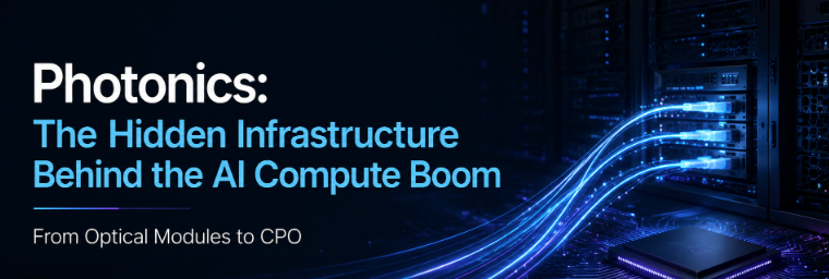
Photonics: The Hidden Infrastructure Behind the AI Compute Boom
After the rapid growth of large AI models and GPU clusters with tens of thousands of cards, the industry has run into a common…
Photonics: The Hidden Infrastructure Behind the AI Compute Boom
After the rapid growth of large AI models and GPU clusters with tens of thousands of cards, the industry has run into a common contradiction: GPU computing power keeps doubling, but a large portion of that power is held back by data transmission bottlenecks. The result is a major pain point across the AI infrastructure stack: idle compute capacity caused by insufficient data movement.
The core answer to this problem lies in photonics, especially optical interconnect technology.
From traditional pluggable optical modules to next-generation CPO, or Co-Packaged Optics, photonics has become an essential infrastructure layer for AI data centers. It has also created a high-growth, high-beta segment within U.S. equities.
This article breaks down the photonics opportunity from four angles: basic principles, industry pain points, technology evolution, and the investment logic behind related U.S.-listed companies.
From an Ave.ai perspective, this is also part of a broader shift: more real-world technology and equity themes are moving on-chain. With Ave.ai, users can explore and trade tokenized stock assets, bringing traditional market opportunities into a faster, more accessible Web3 trading environment.
1. What Does “Light” Mean Inside a Data Center?
A simple way to understand data transmission is to compare it to a logistics system.
Data is the cargo. GPUs are the factories producing computing power. Switches are logistics hubs. Copper cables are ordinary city roads. Optical fiber is a high-speed rail line. Optical modules are the transfer stations that convert between the two transport systems.
Copper vs. Optical Fiber
Copper cables transmit data through electrical signals. They work well over short distances, but their capacity and speed are limited. At high frequencies, signal loss becomes severe, like a road full of traffic lights and potholes.
Optical fiber transmits data through laser photons. It is more like a dedicated high-speed rail line. A single fiber can carry massive bandwidth with very low loss, while supporting much longer distances than copper.
The difference is most visible in three areas:
Transmission capacity: At 200G speeds, copper cables are effective for less than one meter, while optical fiber can easily support tens of meters inside a data center and even long-distance transmission across cities.
Power consumption: Copper requires repeated signal amplification to compensate for loss, which drives up power usage. Optical transmission has much lower energy loss, reducing both electricity costs and cooling pressure.
Cabling density: Copper cable bundles are bulky. A large GPU cluster may require thousands of copper cables, creating severe space and management problems inside racks. Optical fiber is thin and can support more than 1.6T bandwidth per fiber, delivering bandwidth density that is dozens of times higher than copper.
Optical Modules: The “Translator” Between Light and Electricity
GPUs and switch chips cannot directly process optical signals, and electrical signals cannot travel efficiently over long distances through fiber. Optical modules solve this by converting electrical signals into laser signals for fiber transmission, then converting optical signals back into electrical signals at the receiving end.
The principle is similar to home fiber broadband, but the scale is completely different. Home broadband may run at gigabit speeds, while data centers use 800G and 1.6T ultra-high-speed optical modules. The process precision, material requirements, and reliability standards are much higher.
2. Copper Interconnects: A Natural Bottleneck for AI Compute
Traditional cloud data centers mainly handled north-south traffic, meaning traffic between users and servers. Internal communication inside the data center was relatively limited, so copper cables were usually sufficient.
AI training clusters are different. They are dominated by east-west traffic, meaning massive real-time synchronization between GPUs. In a large GPU cluster, internal traffic can be dozens or even hundreds of times greater than that of a traditional data center. This fully exposes the physical limits of copper.
Copper cannot meet AI infrastructure demand because of three unavoidable constraints.
First, copper has a low bandwidth ceiling. A single copper cable has a clear speed limit. Building a large-scale AI cluster would require tens of thousands of copper cables, making rack-level cabling nearly impossible to manage.
Second, copper has limited transmission distance. In high-bandwidth scenarios, signal distortion can occur after only a few meters. This restricts copper mostly to internal server connections and makes efficient communication across racks or cabinets difficult.
Third, copper creates excessive power consumption. To offset high-frequency signal loss, chips need complex compensation circuits. In an AI switch, the copper transmission portion alone can consume tens of watts. At data center scale, this significantly increases electricity and cooling costs.
In simple terms, GPUs are becoming faster, but data transmission is not keeping up. A large amount of compute power is being wasted. The industry trend of “optical replacing copper” has become irreversible.
3. Photonics Technology Evolution: From Pluggable Modules to CPO
The evolution of optical interconnects did not happen in one step. The roadmap can be divided into three generations. These technologies are not simple replacements for each other; they will likely coexist for a long time and serve different use cases.
First Generation: Pluggable Optical Modules
This is currently the most mature and widely used data center solution.
The structure is:
Chip → 20–50 cm PCB copper trace → independent pluggable optical module → optical fiber
Its advantages are clear: high standardization, hot-swappability, and easy maintenance. Today, 800G optical modules are already widely deployed, and 1.6T products are entering the scaling phase.
However, the limitations are also obvious. The electrical signal path is long, which creates signal loss, higher power consumption, and limited bandwidth density. When speeds move toward 3.2T and above, cost and power pressure rise sharply, making this architecture less suitable for future ultra-large AI clusters.
Second Generation: LPO, or Linear Pluggable Optics
LPO is an optimized version of the pluggable architecture. It reduces power consumption by simplifying the driver circuit and lowering signal processing complexity.
Its main advantage is that it keeps the benefits of pluggable modules, such as easier maintenance, while significantly reducing power usage.
LPO is positioned as a cost-effective transition solution. It is expected to gradually penetrate the market around 2026–2027, especially for medium and large compute clusters that need upgrades without fully changing their architecture.
Third Generation: CPO, or Co-Packaged Optics
CPO represents a more fundamental architectural change. It integrates the optical engine directly with the GPU or switch chip on the same substrate using advanced packaging technology.
Using the logistics analogy, CPO is like building the logistics transfer station directly inside the factory warehouse. It removes the road between the factory and the transfer station. Electrical signal routing can shrink from tens of centimeters to less than 10 millimeters, dramatically reducing intermediate loss.
CPO has three major advantages.
First, it can sharply reduce power consumption. Per-port transmission power may fall by 50% to 70%, which can significantly lower AI data center operating costs.
Second, it improves bandwidth density. By integrating many optical channels, a single switch can support several times more bandwidth, enabling 1.6T and 3.2T ultra-high-speed interconnects.
Third, it reduces latency. A shorter optical-electrical conversion path allows GPUs to exchange data faster, improving overall compute utilization.
The general industry consensus is that 2026 will be a small-scale validation period for CPO, while 2027–2028 may mark the beginning of broader commercialization. CPO is widely viewed as a key technology for solving AI interconnect bottlenecks at massive scale.
That said, CPO still faces several commercialization challenges.
Yield: Co-packaging optical devices with high-power chips is technically difficult, and current yields remain a challenge.
Thermal management: Optical components and high-heat chips are packaged together, making cooling significantly more complex.
Maintenance: Once integrated, CPO is not hot-swappable. If one optical component fails, it may not be possible to replace it independently, increasing maintenance costs.

4. U.S. Photonics Supply Chain and Key Stocks
Following the supply-chain bottleneck investing framework, photonics investors should focus first on the most supply-constrained and technically difficult segments of the value chain, rather than simply chasing popular names.
The photonics supply chain can be viewed in four layers:
Upstream materials: InP substrates, silicon photonics wafers, and other core materials.
Core components: Laser chips, modulators, detectors, and other key devices.
Midstream modules: Optical modules, optical engines, packaging, and system manufacturing.
Downstream customers: Switch vendors, NVIDIA, and North American cloud providers.
The following three representative stocks cover three important parts of the chain: upstream materials, midstream optical modules, and CPO laser sources.
Revenue Realization Names: Companies Already Seeing Orders and Revenue
$AXTI: Upstream InP Substrate Leader
AXTI sits at the very upstream end of the photonics industry. It supplies the base substrate material required for high-speed laser chips and optical modules.
AXTI is one of the few companies globally capable of mass-producing large-size InP substrates. It is a typical “picks-and-shovels” company in the AI optical infrastructure boom.
Both current 800G and 1.6T optical modules, as well as future CPO optical engines, require InP substrates. The rapid growth of AI optical modules directly increases demand for these substrates. Because the industry has long faced capacity constraints, expansion across the supply chain can directly support AXTI’s order growth.
$AAOI: Full-Stack Optical Transceiver Manufacturer
AAOI operates in the midstream optical module segment. It covers a full value chain from laser chip manufacturing to optical module packaging and final delivery. Its vertically integrated model, including its own wafer capacity, is relatively rare in the industry.
Its products include 800G and 1.6T data center optical modules, and it is also developing external light source products for CPO-related applications.
Midstream companies like AAOI can have strong earnings leverage during AI demand cycles. Revenue can grow rapidly when demand accelerates, but performance can also be affected by upstream material supply and cloud customer capex cycles.
Catalyst-Driven Names: Technology Is Early, Revenue Has Not Fully Scaled
$SIVE: Core Laser Source Supplier for CPO
SIVE focuses on continuous-wave, or CW, laser sources required for next-generation CPO architecture. These laser sources are key components in CPO systems.
At this stage, CPO is still in the early commercialization phase, and the full market opportunity has not yet been unlocked. Many investors expect CPO-related revenue to accelerate significantly after large-scale adoption begins. This type of small-cap innovation stock offers large long-term upside potential but also comes with very high volatility.
The demand across the photonics supply chain is largely driven by the compute expansion plans of NVIDIA and North American cloud providers. NVIDIA helps define AI cluster interconnect architecture and may also secure upstream laser and optical chip capacity through strategic investments. The strength of AI compute orders directly influences the earnings ceiling of photonics companies.
5. A Beginner Framework for Investing in Photonics Stocks
For beginners, the best starting point is not to chase the hottest stock, but to understand the supply-chain bottlenecks.
The value chain should be viewed from upstream to downstream:
Materials and substrates → optical chips and laser sources → optical modules and systems
Upstream materials often have the highest technical barriers and tightest supply. They may also be more resilient during downturns. Downstream optical module manufacturers face more competition and are more exposed to customer capex cycles.
Why Photonics Stocks Are Highly Volatile
Photonics stocks usually move much more sharply than large-cap blue-chip stocks. There are three main reasons.
First, the sector is highly cyclical. Demand is closely tied to cloud and AI company capital expenditure. If capex slows, earnings pressure can appear quickly.
Second, supply and demand often mismatch. InP substrates and laser chips may require one to two years of capacity expansion. When supply is tight, prices can rise quickly. Once new capacity comes online, pricing pressure may return.
Third, the technology cycle moves fast. The industry is moving from 400G to 800G, 1.6T, and then CPO. Companies that choose the wrong technology path may face valuation pressure for a long time.
A practical research approach is to focus on supply-chain bottlenecks and use financial reports, supply-chain documents, and industry updates to identify gaps between demand and available capacity.
Key indicators to track include:
Order backlogs for upstream substrates and laser chips
AI capex guidance from cloud providers
Commercialization progress of CPO
For everyday investors, useful leading indicators include NVIDIA, Meta, AWS, and other major cloud companies’ AI capex commentary, shipment guidance from leading optical module makers, and capacity expansion progress in upstream core materials.
6. Ave.ai Perspective: From AI Infrastructure Stocks to On-Chain Markets
The photonics sector shows how AI infrastructure is becoming one of the most important investment themes in global markets. As AI data centers scale, opportunities are no longer limited to GPU companies. The value chain now extends into optical modules, laser chips, substrates, packaging, and next-generation interconnect architecture.
This is also where on-chain finance becomes increasingly relevant.
Ave.ai is building a one-stop on-chain finance platform that gives users faster access to market data, trading tools, and tokenized asset opportunities. As tokenized stocks become a larger part of the Web3 financial ecosystem, users can gain exposure to real-world equity themes in a more flexible, on-chain environment.
For traders, this means major market narratives such as AI infrastructure, photonics, tokenized stocks, and DeFi can be connected in one place.
With Ave.ai, users can:
Explore tokenized stock opportunities on-chain.
Track market data and trading activity more efficiently.
Access crypto-native tools for real-world asset exposure.
Move between DeFi markets and tokenized equity themes with greater flexibility.
The long-term direction is clear: traditional finance and on-chain finance are converging. AI infrastructure stocks represent one side of the opportunity. Tokenized stock trading represents the next layer of market access.

Sector Summary and Risk Disclaimer
The competition in AI computing power is also a competition in data transmission capability.
Copper has irreversible physical limitations, while optical interconnects are becoming a long-term structural trend.
In the short term, pluggable optical modules remain the main revenue realization path as 800G and 1.6T products continue to scale.
In the medium to long term, CPO may further expand the industry’s growth ceiling.
The U.S. photonics supply chain covers everything from raw materials to core components and optical modules, giving the sector significant long-term growth potential.
This article is for industry education and market research only. It does not constitute investment advice. U.S. technology stocks can be highly volatile, and investors should fully understand industry cycles, company fundamentals, and individual stock risks before making any investment decisions.
메타데이터
- post_id
- a0ebbc8e7c6e
- slug
- photonics-the-hidden-infrastructure-behind-the-ai-compute-boom-a0ebbc8e7c6e
- url
- https://medium.com/@aveai/photonics-the-hidden-infrastructure-behind-the-ai-compute-boom-a0ebbc8e7c6e
- canonical_url
- https://medium.com/@aveai/photonics-the-hidden-infrastructure-behind-the-ai-compute-boom-a0ebbc8e7c6e
- author_url
- https://medium.com/@aveai
- status
- ok
- fetched_at
- 2026-07-09 05:26:43