Let’s build an external circuit to de-energize parts of our ESP32-H2 setup during deep sleep time…
This tutorial is part of a series of articles about the small ESP32-H2 Super Mini (“SM”) development board. I had actually assumed that I…
Let’s build an external circuit to de-energize parts of our ESP32-H2 setup during deep sleep time to save additional power
This tutorial is part of a series of articles about the small **ESP32-H2 Super Mini (“SM”) development board. I had actually assumed that I would be able to put together the entire project using the measurements of electricity consumption. But then the LoRa UART module threw a wrench in my plans, because its power consumption during deep sleep is far too high for a battery-powered project (see Current measurements of the individual modules of an ESP32-H2 project). In this tutorial I will show you how we can reduce power consumption back into the microampere range using a simple, 3-part circuit**.
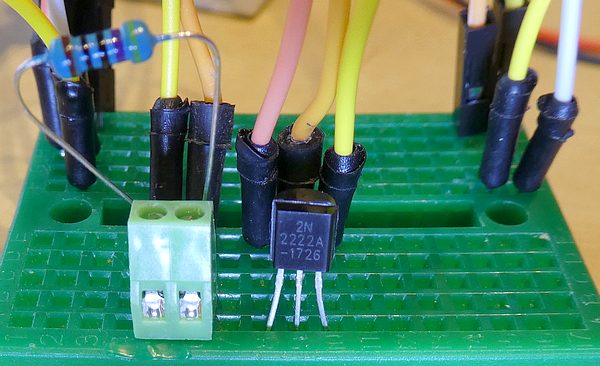
1-stage power switch circuit, Note: the 10K pulldown resistor is missing!
Let’s first take a look at the circuit diagram of the two components:

Simple schematic of a wiring between an ESP32-He Super Mini and a UART-interfaced Lotra module.
Please note that the pins do not correspond to the ones I used for real wiring. The 3.3V output line from the ESP32-H2 is connected to the VCC terminal of the LoRa module, GND is connected to GND, and the two data lines are crossed (TX to RX and RX to TX).
High-side circuit
Therefore, if a larger current still flows during deep sleep, we should follow standard practice and interrupt the 3.3-volt power supply from the ESP32-H2 to the LoRa UART module with a simple circuit (in the schematic above, this is pin 14 to pin 4). Since we want to interrupt the 3.3-volt line to the device, we’re calling this a “high-side” circuit.
We’ll use a “P” MOSFET switch (a good reminder: since we’re interrupting the positive terminal, a P-MOSFET is the appropriate component). We also need a resistor, which we’ll place between the ESP32-H2’s GPIO pin and the MOSFET’s gate to limit the current. The circuit is completed by a resistor between the gate and the 3.3-volt power supply to ensure a defined logic level (a pull-up resistor).

Hide-side power switch with P-MOSFET
In this circuit, we speak of an inverse circuit because when the ESP32-H2’s switching GPIO is set to LOW, the MOSFET switches on and supplies power to the LoRa module. Conversely, as soon as the GPIO is at a high level, the MOSFET interrupts the power supply to the LoRa module.
When selecting a suitable MOSFET, you must ensure that it supports TTL logic (i.e., operates reliably with a signal level of 3.3 volts). I chose the NDP6020P model, which is officially discontinued but still readily available on AliExpress. So much for the theory; now let’s look at the practical side.
I built the circuit and set GPIO pin 1 to LOW before putting the processor into deep sleep. Unfortunately, the result was disappointing, as the current consumption only decreased from 26 mA to 16 mA, but even this figure is still (far) too high. Now we must turn to the second alternative, in which we interrupt the GND line (i.e., “bottom”). This circuit is therefore also called a “low-side” circuit.
Low-side circuit
Basically, we use the same components, but now we have to use an N-MOSFET (we interrupt the negative (or non-) line, hence N-MOSFET; this is pin 8 to pin 5 in the schematic above). The same applies to the N-MOSFET: it must support the TTL logic level. Therefore, in a preliminary version of the circuit, I used a 2N2222A BJT transistor, while in the final circuit, I used an IRLB3034 N-MOSFET.
As with the “high-side” variant, a transistor between the GPIO and the gate of the N-MOSFET limits the switching current, and a “pulldown” resistor between the gate and GND line ensures a defined switching state.

Low-side power switch with N-MOSFET
Similar to the high-side circuit, I connected GPIO 1 to the gate. Before starting deep sleep mode, I set the GPIO to a LOW level, and then comes the moment of truth. In deep sleep mode, I measure the desired current of 0.418 milliamperes, great.

Current meter showing the current measure of 0.418 milliamperes
Pin mapping of a 2N2222A BJT transistor and IRLB3034 N-MOSFET
Updated Feb. 26th, 2026: I only received the N-MOSFET after completing the tutorial, which meant I couldn’t build the circuit until later. I then discovered that the pin assignments for the two types are different:
Use a 2N2222A BJT transistor as a switch
Following the low-side circuit, the current-limiting resistor for the ESP32-H2 processor is connected to the base (B/2 = center) of the transistor. The emitter (E/1 = right) is connected directly to the GND terminal, and the collector (C/3 = left) serves as the GND terminal for our LoRa UART module.

Use an IRLB3034 N-MOSFET as a switch
Now let’s look at the same “low-side” circuit with an N-MOSFET. The connection to the current-limiting resistor for the ESP32-H2 processor is made to the gate (G = left), the source pin (S = right) is connected to GND, and the GND pin of the LoRa UART module is connected to the drain pin (D = center).

This means that the left and middle pins of the two components have a reversed position, so when assembling, pay attention to the correct pins on the component you are using.
Low- vs. High-side circuit
Why did we measure a comparatively high current consumption in high-side mode, even though we disconnected the power supply to the LoRa module? The answer lies in the additional connections between the ESP32-H2 and the LoRa UART module: besides the power supply, there are two additional lines that operate the UART interface (TX and RX lines).
Since we disconnected the power supply to the LoRa module “at the top,” this module draws its power via these GPIOs, causing leakage currents. This is recognizable by the faintly glowing red LED on the LoRa module. An undesirable side effect is that excessive leakage currents can damage the ESP32-H2, as the GPIOs can only handle a maximum current of 20 mA.
Please note that for most externally connected modules, the high-side version is the better option.
Are there ready-made switching modules available?
On the AliExpress platform, you can buy switching modules that promise something like this; for example, this module is priced at 2 euros.

Description: Control can be directly connected to the microcontroller IO. You can use the microcontroller for ARDUINO PWM motor speed control, lamp brightness, and so on. Board use of opto-isolated, completely separated from the 2-terminal voltage. Input is controlled by a 2-pin control; a ground control can be directly connected to the control switch. Control current 1–5 mA control voltage is different; the current difference is mainly the loss on the LED. Charged with maximum current: 22A; more than 5A need to add a heat sink. Board with LED lights. Control can be directly connected to microcontroller IO. The MCU can use ARDUINO PWM to control motor speed and the brightness of lights, and so on. Note that large currents need to add another heat sink.
This module works very well when the switching voltage (i.e., the logic level at the GPIO) is 3.3 volts, but the voltage to be switched (in our case, the supply voltage of the LoRa module) is 5 volts or higher.
Unfortunately, this is not the case with our test setup, because in our circuit the switching voltage and supply voltage are identical at 3.3 volts. In this configuration, the MOSFET installed on the module cannot fully switch on, and only about 1.8 volts are available at the LoRa module, which is far too little for proper operation.
Summary
To use our project with the lowest possible power consumption, the low-side circuit shown above is very suitable and easy to build, even for beginners.
Source code of the app
Please note that I am not providing any standalone sketches for this tutorial, as the measurements already used the existing sketches of the individual modules.
You find the complete code of the other apps and additional material in my GitHub repository “**ESP32_H2_Super_Mini_LoRa_Transmitter_Project**”.
Happy coding!
메타데이터
- post_id
- a1ec6de43cf7
- slug
- lets-build-an-external-circuit-to-de-energize-parts-of-our-esp32-h2-setup-during-deep-sleep-time-a1ec6de43cf7
- url
- https://medium.com/@androidcrypto/lets-build-an-external-circuit-to-de-energize-parts-of-our-esp32-h2-setup-during-deep-sleep-time-a1ec6de43cf7
- canonical_url
- https://medium.com/@androidcrypto/lets-build-an-external-circuit-to-de-energize-parts-of-our-esp32-h2-setup-during-deep-sleep-time-a1ec6de43cf7
- author_url
- https://medium.com/@androidcrypto
- status
- ok
- fetched_at
- 2026-06-09 15:37:30