FPGA Development from Scratch: Complete Vivado Step by Step Guide for Beginners…
Mastering Vivado: Your Complete FPGA Development Roadmap
FPGA Development from Scratch: Complete Vivado Step by Step Guide for Beginners (Verilog-Vivado-Nexys A7 Artix 7 FPGA Board)
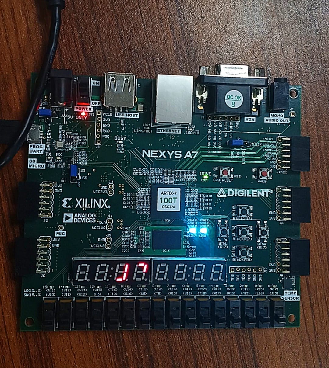
Mastering Vivado: Your Complete FPGA Development Roadmap
Stepping into the world of Field-Programmable Gate Arrays (FPGAs) can feel like entering a foreign country where the language is hardware, the currency is logic gates, and the map is a complex toolchain. Unlike traditional software programming, FPGA development requires thinking in parallel, understanding physical constraints, and mastering sophisticated development environments.
This comprehensive guide will transform you from an FPGA beginner to a confident developer using Xilinx Vivado and the Nexys A7 Artix-7 board. We’ll walk through every step. From creating your first project to deploying on actual hardware with detailed explanations and practical examples.
Understanding the FPGA Development Mindset
The Fundamental Shift: Software vs Hardware Thinking
Software: Sequential execution, variables, functions
Hardware: Parallel execution, signals, modules
Key Mindset Changes:
- Everything happens simultaneously: All always blocks run in parallel
- Time matters: Physical delays and timing constraints are critical
- Resources are finite: Every LUT and flip-flop counts
- Synthesis is compilation: Your code becomes actual hardware
The Complete Development Flow
Idea → RTL Coding → Simulation → Synthesis → Implementation → Bitstream → Hardware
   ↑          ↑           ↑          ↑             ↑           ↑          ↑
Planning   Writing     Testing   Converting    Placing &   Generating  Deploying
           Code        Logic     to Gates      Routing     File        on FPGA
Step 1: Project Planning & Setup
Choosing Your Development Environment
- Tool: Xilinx Vivado Design Suite (WebPACK edition is free)
- Board: Digilent Nexys A7 with Artix-7 FPGA
- HDL: Verilog (our focus for this guide)
- Target Part: XC7A100T-1CSG324C
Pre-Development Checklist
~Install Vivado with Artix-7 device support ~Connect Nexys A7 board and install drivers ~Understand basic Verilog syntax ~Gather documentation for your FPGA board ~Set up workspace with organized folder structure
Step 2: Creating Your First Vivado Project
Launching and Initial Setup
- Open Vivado and select Create Project from Quick Start
- Click Next to begin the project creation wizard
- Project Name: Choose a descriptive name (e.g.,
led_blinker) - Project Location: Select a dedicated workspace directory
- Project Type: Select RTL Project and check Do not specify sources at this time
Project Type Deep Dive
RTL Project: Most common - you write Register Transfer Level code
Post-Synthesis Project: Work with synthesized netlists
I/O Planning Project: Focus on pin planning before coding
Imported Project: Import existing projects
Selecting the Target FPGA
- Click Boards tab and search for “Nexys A7”
- Select Nexys A7–100T from the list
- Alternatively, use Parts tab and manually select:
- Family: Artix-7
- Package: csg324
- Speed: -1
- Filter: xc7a100tcsg324–1 (Last Option)
Personal Tip: Using the Boards option automatically configures many settings and constraints specific to your hardware.
Step 3: Verilog Coding Fundamentals
Understanding the Module Structure
module module_name (
    // Port declarations
    input wire clock,
    input wire reset_n,  // _n indicates active-low
    input wire [7:0] data_input,
    output reg [7:0] data_output,
    output wire ready
);
    // Internal signal declarations
    reg [7:0] internal_register;
    wire combinatorial_signal;

    // Module functionality
    always @(posedge clock) begin
        if (!reset_n) begin
            internal_register <= 8'b0;
        end else begin
            internal_register <= data_input;
        end
    end

    assign data_output = internal_register;
    assign ready = (internal_register != 0);

endmodule
Essential Verilog Concepts (Must knows)
Data Types
- wire: Represents physical connections, used for combinational logic
- reg: Represents storage elements, used in always blocks
- parameter: Constants for code flexibility
Always Blocks
// Combinational logic - sensitive to input changes
always @(*) begin
    output = input1 & input2;
end
// Sequential logic - sensitive to clock edges
always @(posedge clock) begin
    if (reset)
        counter <= 0;
    else
        counter <= counter + 1;
end
Blocking vs Non-Blocking Assignments
// Blocking (=) - sequential execution (avoid in sequential logic)
a = b;
c = a;  // c gets new value of a
// Non-blocking (<=) - parallel execution (use in sequential logic)
a <= b;
c <= a; // c gets old value of aStep 4: Writing Effective Testbenches
Testbench Architecture
module tb_your_design;
    // Inputs (declared as reg)
    reg clk;
    reg reset;
    reg [3:0] test_input;

    // Outputs (declared as wire)
    wire [3:0] test_output;
    wire status_signal;

    // Clock generation
    always #5 clk = ~clk;  // 100MHz clock

    // Instantiate Unit Under Test (UUT)
    your_design uut (
        .clk(clk),
        .reset(reset),
        .data_in(test_input),
        .data_out(test_output),
        .status(status_signal)
    );

    // Test sequence
    initial begin
        // Initialize signals
        clk = 0;
        reset = 1;
        test_input = 4'b0000;

        // Release reset
        #100 reset = 0;

        // Test case 1: Normal operation
        test_input = 4'b1010;
        #100;

        // Test case 2: Edge case
        test_input = 4'b1111;
        #100;

        // Add more test cases...

        #1000 $finish;
    end

    // Monitoring and debugging
    initial begin
        $monitor("Time: %0t | Input: %b | Output: %b",
                 $time, test_input, test_output);
    end
endmodule
Advanced Testbench Techniques
// File I/O for test vectors
initial begin
    integer file, value;
    file = $fopen("test_vectors.txt", "r");
    while (!$feof(file)) begin
        $fscanf(file, "%b", value);
        test_input = value;
        #100;
    end
    $fclose(file);
end
// Automated verification
always @(test_output) begin
    if (test_output === expected_value)
        $display("PASS: Output matches expected");
    else
        $display("FAIL: Got %b, Expected %b", test_output, expected_value);
end
Step 5: Simulation & Debugging
Running Behavioral Simulation
- Flow Navigator → Simulation → Run Simulation → Behavioral Simulation
- Vivado launches the simulator with waveform view
- Add signals to waveform window by dragging from Scope window
- Run for specific time or until completion
Waveform Analysis Techniques
- Zoom controls: Fit to window, zoom in/out for detailed timing
- Cursor measurements: Check signal timing relationships
- Signal groups: Organize related signals together
- Radix settings: Display signals as binary, hex, decimal, or analog
Common Simulation Tasks
// Debugging with $display
always @(posedge clk) begin
    $display("Cycle: %0d | State: %b | Output: %h",
             cycle_count, current_state, data_output);
end
// Conditional breakpoints
always @(posedge clk) begin
if (data_output === 8'hFF) begin
$display("Breakpoint hit at time %0t", $time);
$stop;
end
endStep 6: Constraints File (.xdc) Mastery
Understanding Constraints
# Clock definition
set_property PACKAGE_PIN E3 [get_ports clk]
set_property IOSTANDARD LVCMOS33 [get_ports clk]
create_clock -add -name sys_clk_pin -period 10.00 -waveform {0 5} [get_ports clk]
# Input buttons/switches
set_property PACKAGE_PIN C12 [get_ports reset]
set_property IOSTANDARD LVCMOS33 [get_ports reset]
set_property PACKAGE_PIN J15 [get_ports {data_in[0]}]
set_property IOSTANDARD LVCMOS33 [get_ports {data_in[0]}]# Output LEDs
set_property PACKAGE_PIN H17 [get_ports {leds[0]}]
set_property IOSTANDARD LVCMOS33 [get_ports {leds[0]}]# Timing exceptions (if needed)
set_false_path -from [get_ports {async_input}]Constraint Types Explained
- I/O Constraints: Pin locations and electrical standards
- Timing Constraints: Clock definitions and timing exceptions
- Physical Constraints: Placement and routing guidance
- Configuration Constraints: Bitstream generation options
Step 7: Synthesis & Implementation
Running Synthesis
- Flow Navigator → Synthesis → Run Synthesis
- Monitor progress in Console window
- Review Synthesis Report for:
- Resource utilization (LUTs, FFs, BRAM, DSP)
- Timing estimates (worst negative slack)
- Warnings and critical warnings
Implementation (Place & Route)
- Flow Navigator → Implementation → Run Implementation
- Analyze Implementation Reports:
- Timing Summary: Check setup/hold violations
- Utilization: Verify resource usage
- Power: Estimate power consumption
Step 8: Bitstream Generation & Hardware Deployment
Generating the Programming File
- Flow Navigator → Program and Debug → Generate Bitstream
- Wait for process to complete (5–15 minutes typically)
- Check for critical warnings in messages
Bitstream Options
# Additional bitstream settings in .xdc
set_property BITSTREAM.CONFIG.SPI_BUSWIDTH 4 [current_design]
set_property CFGBVS VCCO [current_design]
set_property CONFIG_VOLTAGE 3.3 [current_design]
Hardware Setup & Programming
- Connect Nexys A7 via USB cable to laptop/PC
- Power on the board (switch near USB connector)
- Open Hardware Manager (Flow Navigator)
- Auto Connect to detect your board
- Program Device with generated .bit file
Programming Methods
- JTAG: Temporary programming (lost on power cycle)
- Flash: Permanent programming (survives power cycle)
- Debug Probes: Integrated Logic Analyzer (ILA) for live debugging
Step 9: On-Board Verification & Debugging
Hardware Testing Protocol
- Basic functionality: Verify inputs and outputs work
- Timing verification: Check real-world timing behavior
- Stress testing: Test edge cases and boundary conditions
- Long-term stability: Run for extended periods
Step 10: Best Practices & Optimization
Coding Guidelines
- Use meaningful signal names that indicate purpose
- Group related signals into buses when possible
- Comment complex logic and state machine transitions
- Parameterize values that might need adjustment
Timing Closure Strategies
- Register all outputs to improve timing
- Use pipeline stages for long combinational paths
- Balance logic levels across critical paths
- Consider clock enabling instead of clock division
Resource Optimization
// Use shared resources
module resource_sharing_example (
    input [7:0] a, b,
    input sel,
    output [7:0] result
);
    // Instead of separate adders, use one with mux
    wire [7:0] add_result = a + b;
    wire [7:0] sub_result = a - b;
    assign result = sel ? add_result : sub_result;
endmodule
Common Pitfalls & How to Avoid Them
Simulation-Synthesis Mismatches
// Simulation works, hardware doesn't:
reg [3:0] counter;
always @(posedge clk) begin
    counter = counter + 1;  // Should use <= for sequential
end
// Fix: Use non-blocking for sequential logic
always @(posedge clk) begin
    counter <= counter + 1;
end
// Fix: Add default case
default: out = 0;
Clock Domain Crossing Issues
// Unsafe crossing between clock domains
always @(posedge clk_b) begin
    signal_b <= signal_a;  // Metastability risk
end
// Safe crossing: Use synchronizer chain
reg [2:0] sync_chain;
always @(posedge clk_b) begin
    sync_chain <= {sync_chain[1:0], signal_a};
end
assign safe_signal = sync_chain[2];
Conclusion: Your FPGA Journey Begins
Mastering Vivado and FPGA development opens doors to creating custom digital systems with unparalleled flexibility and performance. The journey from concept to working hardware involves many steps, but each one builds your understanding of digital design principles.
Remember that FPGA development is iterative and expect to go through the design flow multiple times as you debug and optimize your designs. The skills you’ve learned here form the foundation for increasingly complex projects, from simple LED blinkers to sophisticated digital signal processing systems.
The most important next step is practice. Start with simple projects, gradually increase complexity, and don’t be afraid to experiment. Every design even if successful or not, teaches valuable lessons about hardware complexities and programming concepts.
메타데이터
- post_id
- a66989ffd8b1
- slug
- fpga-development-from-scratch-complete-vivado-step-by-step-guide-for-beginners-a66989ffd8b1
- url
- https://medium.com/@smhashaam/fpga-development-from-scratch-complete-vivado-step-by-step-guide-for-beginners-a66989ffd8b1
- canonical_url
- https://medium.com/@smhashaam/fpga-development-from-scratch-complete-vivado-step-by-step-guide-for-beginners-a66989ffd8b1
- author_url
- https://medium.com/@smhashaam
- status
- ok
- fetched_at
- 2026-07-15 12:57:07