Substrate Noise Coupling in Deep Submicron Mixed-Signal ICs
Vansh Parate, Anirudh Nurani, Amar Ware EXTC, Sardar Patel Institute of Technology Date: April 15, 2026
Substrate Noise Coupling in Deep Submicron Mixed-Signal ICs
Vansh Parate, Anirudh Nurani, Amar Ware EXTC, Sardar Patel Institute of Technology Date: April 15, 2026
Mentor: Prof. Najib Ghatte Co-Mentor: Prof. Sneha Weakey
Abstract
As CMOS technology progresses to smaller scales, integrating both high-speed digital circuits and accurate analog circuits on a single die has become very popular among modern mixed-signal devices. Unfortunately, this leads to many problems related to noise coupling via the silicon substrate between analog and digital parts, because switching activities in digital cells result in the injection of noise into the silicon substrate.
The propagation of noise along resistive and capacitive substrate paths has a harmful effect on various sensitive analog devices such as ADCs, PLLs, voltage references, and RF front-ends. The problem gets worse as CMOS processes evolve and reach the deep-submicron level because of the increase in speed, decrease in supply voltage, and increase in device density.
In this paper, we discuss the physics of substrate noise, examine its effect on performance, and analyze various substrate noise control solutions, from guard rings and deep N-well isolation to differential techniques and advanced floorplanning methods.
1. Introduction
The development of CMOS technology up to deep submicron levels (90 nm, 65 nm, 28 nm and below) has enabled integration of high-speed digital and analog circuits on a single silicon die. This integration is important for the development of SoCs used in communications, IoT, biomedical electronics, and consumer systems.
However, the inclusion of digital circuits that are inherently noisy into an analog system creates a problem of substrate noise coupling, which must be analyzed carefully.
Substrate noise coupling refers to a phenomenon where noise generated by digital circuits through switching operations propagates through a shared substrate and contaminates the analog part of the chip. The effect is amplified by higher transistor densities, faster switching operations, and low supply voltages associated with deep submicron technologies.
1.1 Background
Earlier, analog and digital circuits were implemented on separate chips, reducing interference issues.
With the introduction of mixed-signal ASICs in the 1990s and early 2000s:
- Digital circuits operated at lower speeds
- Supply voltages were higher
- Device density was relatively low
Thus, substrate effects were considered secondary.
However, with deep submicron scaling:
- Switching frequency increased significantly
- Supply voltage dropped below 1V
- Device density increased
- Isolation margins reduced
As a result, analog circuits became highly sensitive to substrate effects, leading to:
- Increased jitter in PLLs
- ADC distortion
- Degraded RF front-end performance
To address these challenges, techniques such as substrate modeling, guard rings, deep N-well isolation, and differential signaling are used.
1.2 Research Questions
The study is guided by the following questions:
- How does digital switching impact sensitive analog circuits in deep submicron mixed-signal ICs?
- How do substrate isolation methods relate to signal quality improvement?
- What role does technology scaling play in substrate noise propagation?
- How effective are layout-level and circuit-level mitigation techniques?
2. Literature Review
A review of existing scholarly work ensures the study is grounded in established theory.
- High-resistivity silicon has been shown to reduce substrate noise coupling in advanced nodes such as 28 nm FD-SOI.
- Industry studies highlight the importance of noise reduction in mixed-signal ASIC design.
These works confirm that substrate noise mitigation is a critical requirement in modern IC design.
3. Methodology
The research approach is analysis-based and involves simulation and literature review to identify substrate noise effects and mitigation techniques.
3.1 Data Collection
Data sources include:
- Peer-reviewed journal articles
- Conference papers
- Semiconductor industry white papers
- Comparative studies across technology nodes
Collected parameters include:
- Switching frequencies
- Supply voltages
- Substrate noise levels
- Analog performance degradation metrics
- Effectiveness of isolation techniques
Mathematical models representing the substrate as a distributed RC network were also analyzed.
3.2 Analysis Framework
1. Mechanism Analysis
Coupling Mechanism
Noise generation mechanisms were categorized as:
- Resistive coupling
- Capacitive coupling
- Ground bounce and supply noise interaction
These were studied using semiconductor physics concepts such as resistivity, parasitic capacitance, and transient current behavior.
2. Technology Scaling Comparison
The impact of scaling was analyzed in terms of:
- Supply voltage reduction
- Increased switching speed
- Increased device density
3. Mitigation Techniques Evaluation
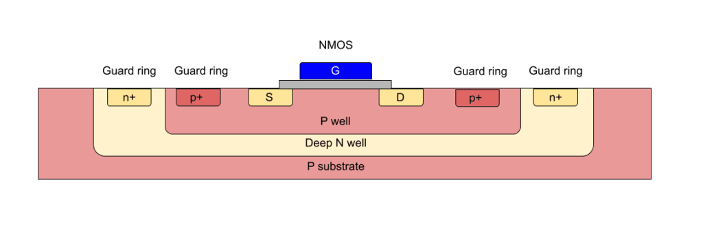
Techniques were evaluated based on:
- Noise reduction capability
- Complexity
- Area overhead
- Compatibility with modern CMOS
Methods studied include:
- Guard rings
- Deep N-well isolation
- Differential signaling
- Floorplanning
4. Performance Degradation Evaluation
Performance was analyzed using:
- Phase noise
- Clock jitter
- Signal-to-noise ratio
- Effective number of bits
4. Results
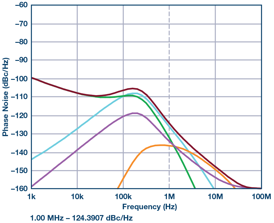
Observation 1
The speed of digital signals is directly proportional to substrate noise amplitude.
Observation 2
Technology scaling worsens substrate coupling due to reduced isolation and increased density.
Observation 3
Isolation methods significantly reduce substrate noise but introduce area and complexity overhead.
Observation 4
Performance degradation is observed in:
- Increased phase noise
- Higher clock jitter
- Reduced SNR
- Lower ENOB
The results indicate a strong correlation between digital switching activity and analog performance degradation.
6. Conclusion
Efficient suppression of substrate noise requires a combination of:
- Physical isolation techniques
- Layout optimization
- Noise-tolerant circuit design
Differential circuits are particularly effective in reducing common-mode noise.
A multi-level approach is necessary to maintain signal integrity in mixed-signal ICs.
Understanding substrate noise is essential for designing reliable systems such as ADCs, PLLs, RF front ends, and other precision analog circuits integrated within digital SoCs.
Future work includes exploration of:
- Silicon-on-Insulator (SOI) technologies
- 3D IC design challenges
- Adaptive noise suppression techniques
References
- Karipidis et al. (2023) — Substrate coupling simulation for mobile SoC
- Arora & Menon (2023) — Substrate noise challenges in nano-CMOS
- D’Souza (2023) — Supply interference impact on analog circuits
메타데이터
- post_id
- a83174877a33
- slug
- substrate-noise-coupling-in-deep-submicron-mixed-signal-ics-a83174877a33
- url
- https://medium.com/@vansh.parate24/substrate-noise-coupling-in-deep-submicron-mixed-signal-ics-a83174877a33
- canonical_url
- https://medium.com/@vansh.parate24/substrate-noise-coupling-in-deep-submicron-mixed-signal-ics-a83174877a33
- author_url
- https://medium.com/@vansh.parate24
- status
- ok
- fetched_at
- 2026-07-19 21:53:32