Implementing a 3×3 2D Image Filter in VHDL
Applying a 3×3 filter to an image can be thought of as the “hello world” of FPGA image processing. You can perform operations such as…
Implementing a 3×3 2D Image Filter in VHDL
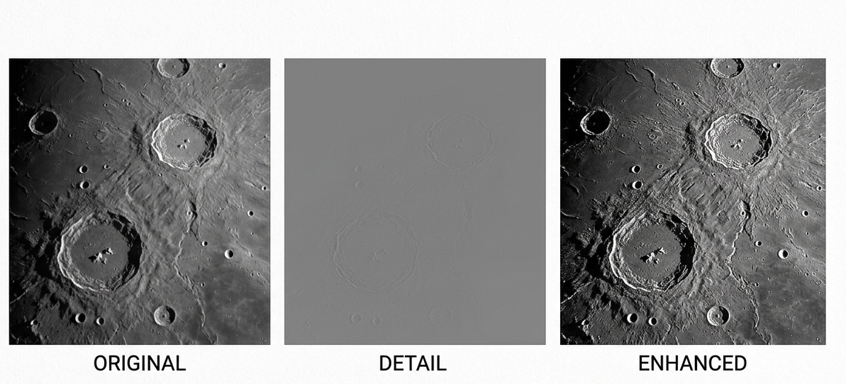
Applying a 3×3 filter to an image can be thought of as the “hello world” of FPGA image processing. You can perform operations such as blurring, sharpening, edge detection, Sobel, and Laplacian filtering on images. They all boil down to a small core problem: “For each output pixel, you need the current pixel plus its 8 neighbors.”
In this post, we will examine how to design an optimized 3×3 filtering structure on an FPGA with minimal resource utilization.
Most FPGA video pipelines use the AXI Stream protocol. In this protocol, one pixel is provided at each clock cycle when valid signal asserted, and the system has a backpressure option using the ready signal. At the beginning of a video frame, the protocol’s tuser bit is asserted, and at the end of each line, the system’s tlast signal is asserted. For more details, see: https://docs.amd.com/r/en-US/ug1399-vitis-hls/How-AXI4-Stream-Works

From the picture above, you can see that the first pixel, (1,1), arrives at the start of the frame with the tuser signal asserted. Pixels (1,2), (1,3), and so on follow until the end of the line, where the tlast signal is asserted. The second line follows the same pattern.
To generate the first valid output pixel, data from the first two lines and the first three pixels of the third line are required to perform the filter multiplication (In this work, we will not perform padding). Note that this is not a matrix multiplication; instead, it is an element-wise multiplication between the pixel values and the filter coefficients, followed by an accumulation of the results.
The filter computation can therefore be expressed as follows:


Consequently, a minimum of two line buffers is required for the first and second image lines, with each buffer sized to accommodate one full image line. Additionally, a controller is nedeed to manage the incoming data streams into the FIFOs as well as the outgoing data streams from the FIFOs. Therefore, the proposed system architecture, including the FIFO buffers and the controller managing the AXI-Stream interfaces, is illustrated in the figure below:

The proposed architecture implements a fully streaming 3×3 image filtering structure using two FIFO-based line buffers and a central controller. Pixel data enters the system through the input stream and is written into FIFO 1, which delays the data by one image line, while FIFO 2 cascades this delay to provide pixel data from two lines earlier. The controller controls both the read and write operations of the FIFOs, ensuring proper data flow and alignment using tlast and tuser signals. Then, it simultaneously receives the current line, the one-line-delayed stream, and the two-line-delayed stream, allowing it to align three vertically adjacent pixels in real time. Using internal pipeline registers, the controller constructs the required 3×3 neighborhood, performs element-wise multiply–accumulate operations with the filter coefficients, and generates the filtered output stream while preserving AXI-Stream frame (tuser) and line (tlast) signaling. Since performing nine multiplications and summing them within a single clock cycle would violate timing constraints at high pixel rates, the multiplication and accumulation operations are distributed across multiple pipeline stages, enabling the design to meet the desired clock frequency while maintaining a throughput of one output pixel per clock in steady state.
The proposed pipelined architecture operates with a throughput of one input sample per clock cycle and one output sample per clock cycle once the pipeline is filled.
After implementation, using FIFO buffers with a depth of 4096, the system utilized 3 DSP blocks, 3 BRAMs, and 523 LUTs when implemented on a Xilinx UltraScale+ FPGA. Timing analysis shows that the design can operate at a maximum clock frequency of 330 MHz when the FPGA is otherwise unoccupied.
메타데이터
- post_id
- b5fcbea00995
- slug
- implementing-a-3-3-2d-image-filter-in-vhdl-b5fcbea00995
- url
- https://medium.com/@alperenbalci/implementing-a-3-3-2d-image-filter-in-vhdl-b5fcbea00995
- canonical_url
- https://medium.com/@alperenbalci/implementing-a-3-3-2d-image-filter-in-vhdl-b5fcbea00995
- author_url
- https://medium.com/@alperenbalci
- status
- ok
- fetched_at
- 2026-07-15 20:55:46