Protect Your 3D IC Designs from ESD Threats
3D ICs have emerged as the industry’s answer to Moore’s Law slowdown, connecting and stacking dies to achieve performance once thought…
Protect Your 3D IC Designs from ESD Threats
3D ICs have emerged as the industry’s answer to Moore’s Law slowdown, connecting and stacking dies to achieve performance once thought impossible.
2.5D interposers and TSV-based 3D architectures now power breakthroughs in AI, high-performance computing, and automotive electronics.

Figure 1. 3D IC stack (Source: incompliancemag.com)
But as chips merge into complex vertical systems, new risks surface: thermal gradients, mechanical stress, reliability degradation, and ESD vulnerabilities. Each layer interacts, each interconnect matters, and understanding these multi-physics effects has become the key to reliable 3D design.
Understanding Electrostatic Discharge (ESD) in 3D Designs
Electrostatic discharge (ESD) is the instantaneous release of stored electrical charge. In today’s nanometer-scale devices, even a transient of a few volts — or tens of volts — can permanently damage delicate transistor structures.
Compared with traditional packaging, ESD risks in advanced packaging grow exponentially as ESD discharge paths have become unpredictable, rendering conventional protection schemes less effective. The major challenges include:
- Uncontrolled current paths: ESD current is no longer confined within a single die. During discharge, it may travel across multiple dies, interposers, or substrates — bypassing on-chip ESD protection circuits and directly damaging vulnerable interconnect structures.
- Fragile micro-interconnects: Micro-bumps (μ-bumps), TSVs, and hybrid bonding interfaces are only a few microns in size, with very limited cross-sectional area and low current-carrying capacity (It₂). Traditional ESD circuits are difficult to scale to such miniature geometries. Under high ESD surge, these fine structures behave almost like “fuses,” easily melting or breaking down.
- Potential imbalance in heterogeneous integration: Different dies within a package operate at different voltages and ground references. For example, in case a 3nm logic die stacked with a DRAM die on a mature node, each technology exhibits different ESD tolerance levels and process characteristics. During a nanosecond-scale ESD event, transient ground potential differences can form unintended discharge paths between dies.
- System-level capacitance effects: The complex 3D structure alters the overall capacitance characteristics of the package, significantly impacting how CDM (Charged Device Model) ESD events occur — their magnitude, polarity, and discharge path — making them harder to predict and protect against.
Among various ESD models — HBM (Human Body Model), MM (Machine Model), and particularly CDM — CDM poses the greatest threat.
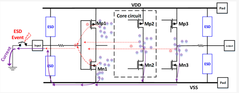
Figure 2. In a classic CDM ESD protection scheme, due to random internal charge storage, the charges will run through the internal chip en route to discharge into a grounding pad. (Source: Electronics 2024)
In automated handling and testing environments, large and complex package assemblies are more prone to accumulating charge and releasing it abruptly, resulting in severe CDM-induced damage.
Cross-Domain Power and Voltage Management
In 2.5D and 3D architectures, each chiplet may operate at a different voltage or power domain. This cross-domain environment increases design complexity and poses additional ESD risks.
An ESD pulse in one voltage domain can propagate across inter-die connections and damage other dies. Designers must therefore build cross-domain ESD protection circuits that suppress discharge without degrading normal signal integrity. Achieving this balance often requires sophisticated co-design strategies and customized protection networks.
Heat and Reliability: The Thermal Dimension of ESD
The stacked nature of 3D ICs makes heat dissipation more difficult, raising junction temperatures during operation. Elevated temperatures can alter ESD device characteristics — lowering breakdown voltage, increasing on-resistance, and reducing protection efficiency.
Thermal expansion also introduces mechanical stress in TSVs and micro bumps, potentially impacting long-term reliability. Effective ESD design in 3D ICs therefore requires co-optimization of thermal management, materials, and protection devices, ensuring stability even in high-temperature environments.
System-Level ESD Co-Optimization
Multi-die systems often combine chips from different design teams or suppliers, making ESD co-design particularly challenging. Protection circuits must work in concert across dies to prevent discharge propagation and avoid mismatched behavior. System-level modeling that accounts for inter-die delay, parasitics, and signal coupling is essential to optimize ESD strategies holistically rather than die-by-die.
This approach requires involving chip designers, packaging engineers, and OSAT vendors early in the project, treating the entire package system as a unified whole for ESD protection planning, and collaboratively defining grounding strategies and discharge current paths.
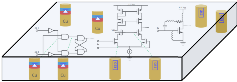
Figure 3. Internally distributed CDM ESD protection using vertical in-TSV ESD protection devices (Source: Micromachines)
In the past, ESD protection for external I/Os was mostly implemented directly on the chip itself, consuming valuable die area and driving up cost. The requirements are also tightening — from around 30 V down to 5 V (or even lower). As interfaces multiply and layout density increases, the target must drop to 5 V or below. Each interface needs roughly 1 µm² of area for ESD protection, and with hundreds or thousands of I/Os, the protection circuits quickly consume the available silicon real estate. This is the essence of ESD scaling: more interfaces, less space, and inevitably lower protection margins — a growing challenge for next-generation designs.
Now, there’s a smarter alternative: shifting part of the I/O ESD protection onto the TSV Interposer. With their fast response time and high energy absorption capability, TVSs can effectively clamp transient voltages and isolate voltage domains during an ESD strike. High-density TVS arrays or micro-scale TVS components allow designers to achieve compact, high-efficiency protection, reducing the risk of ESD propagation throughout the system.
Paving the Way for Reliable 3D IC Innovations
Designing ESD protection for 2.5D and 3D ICs is one of the most complex tasks in modern chip engineering.
Looking ahead, as the chiplet ecosystem matures and the number of 3D stacking layers continues to increase, the complexity of electrostatic discharge (ESD) management will only intensify . By adopting system-level ESD design and collaborating across the entire value chain can we ensure the reliability and success of the next generation of heterogenous multi-chiplet systems.
메타데이터
- post_id
- bb5f3be90ef9
- slug
- protect-your-3d-ic-designs-from-esd-threats-bb5f3be90ef9
- url
- https://medium.com/@emsyan/protect-your-3d-ic-designs-from-esd-threats-bb5f3be90ef9
- canonical_url
- https://medium.com/@emsyan/protect-your-3d-ic-designs-from-esd-threats-bb5f3be90ef9
- author_url
- https://medium.com/@emsyan
- status
- ok
- fetched_at
- 2026-07-26 06:49:41