Accelerating Trillion-Parameter AI Models with NVIDIA Blackwell GPUs and the GB200 NVL72 Cluster
Nvidia Blackwell GPUs and rack-scale GB200 NVL72: Key Architecture Innovations and Specifications.
Accelerating Trillion-Parameter AI Models with NVIDIA Blackwell GPUs and the GB200 NVL72 Cluster
NVIDIA’s latest announcement reveals that training an AI model with 1.8 trillion parameters, akin to the scale of OpenAI’s GPT-4, would require just 2,000 Blackwell GPUs and consume only 4 megawatts of electricity. This marks a substantial improvement over the previous Hopper GPU technology, which needed 8,000 GPUs and 15 megawatts for the same task. In this blog post, we delve into the key architectural innovations of the Blackwell GPUs and explore the specifications of the newly introduced Blackwell GPU systems.
Blackwell Architecture Innovations
NVIDIA’s Blackwell GPUs (B100/200) feature the following advancements:
- AI Superchip with 208 Billion Transistors
- 2nd Generation Transformer Engine
- 5th Generation NVLink Interconnect
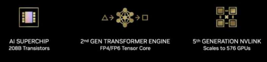
AI Superchip with 208 Billion Transistors
The AI Superchip in the Blackwell architecture integrates a staggering 208 billion transistors and utilizes a specialized TSMC 4NP process for manufacturing. This design includes two reticle-limited dies connected via a high-speed 10 terabytes per second (TB/s) chip-to-chip interconnect. This configuration results in an unprecedented compute capability of near 20 PFLOPS (FP4) on a single chip. The superchip integrates 8 stacks of 8-hi HBM3e with up to 192GB capacity operating at 8TB/s.
The term “reticle-limited die” describes the maximum die size achievable within the constraints of the reticle, or photomask, used in photolithography — the process of projecting circuit patterns onto a silicon wafer.
![Blackwell GPU superchip (B100 or B200) [1]](https://miro.medium.com/v2/resize:fit:449/1*-4-YAmdrKcE4b6Jp-sO9EQ.png)
Blackwell GPU superchip (B100 or B200) [1]
2nd Generation Transformer Engine
The Blackwell Transformer Engine supports Microscaling (MX) data formats such as MXFP4, MXFP6, MXFP8, and MXINT8. Recent research by Microsoft demonstrated that training with MXFP4 weights and MXFP6 activations and gradients results in a minor loss penalty for generative language models, while MXFP6 closely matches FP32 for inference after quantization-aware fine-tuning.
5th Generation NVLink Interconnect
Blackwell GPUs are equipped with 18 fifth-generation NVLink links, delivering a total bidirectional bandwidth of 1.8 TB/s, compared to Hopper’s maximum of 900 GB/s. Building on this, NVIDIA has developed a multi-server cluster system utilizing the NVIDIA NVLink Switch, designated as GB200 NVL72. This configuration dramatically elevates the network bandwidth to 130 TB/s, 72 times 1.8 TB/s, effectively linking 72 GPUs within a single NVLink zone.
Blackwell HGX
Blackwell HGX extends the existing HGX system to include Blackwell GPUs replacing H100 or A100 GPUs.
HGX B100 is a x86 platform based on 8 B100 GPU baseboards, offering 112 PetaFLOPS in FP4, and a drop-in replacement for existing H100 HGX infrastructures. Each B100 GPU can be configured to consume up to 700W.
HGX B200 is a x86 platform based on 8 B200 GPUs, offering 144PetaFLOPS in FP4. Each B200 GPU can be configured to consume up to 1000W.
NVIDIA B200 vs AMD MI300X
The NVIDIA B200 outperforms AMD’s MI300X in processing power, delivering 4.5 PFLOPS in dense computations and 9 PFLOPS in sparse computations at 8-bit precision. In contrast, the MI300X processes 2.61 PFLOPS in dense computations and 5.22 PFLOPS in sparse computations at the same precision. Additionally, the B200 features a peak memory bandwidth of 8TB/s, compared to the 5.3TB/s offered by the MI300X. Both B200 and MI300X are equipped with 192GB of HBM memory.
![HGX B200 versus HGX B100 [3]](https://miro.medium.com/v2/resize:fit:1088/1*kZ5KA--QlboVrobwX-fYug.png)
HGX B200 versus HGX B100 [3]
![B200 (left) versus B100 (right) [3]](https://miro.medium.com/v2/resize:fit:1094/1*0RTO3WDUzc4MVKhVObUuBA.png)
B200 (left) versus B100 (right) [3]
GB200 Superchip
The NVIDIA GB200 Grace Blackwell superchip features an integrated design consisting of one Grace CPU and two B200 GPUs. The NVLink-C2C interconnect provides an aggregate bidirectional bandwidth of 900GB/s from the Grace CPU to the two B200 GPUs, allowing them to access Grace CPU’s LPDDR5X memory seamlessly.
![Grace Blackwell Superchip (GB200) featuring two Blackwell GPUs and one Grace CPU [1]](https://miro.medium.com/v2/resize:fit:403/1*TT9yRAk5ogpzEOxnaxjAlQ.png)
Grace Blackwell Superchip (GB200) featuring two Blackwell GPUs and one Grace CPU [1]
![Grace Blackwell Superchip (GB200) Spec [3]](https://miro.medium.com/v2/resize:fit:580/1*MtDOzGkzI7NHJLkxvn8zgQ.png)
Grace Blackwell Superchip (GB200) Spec [3]
GB200 NVL72 Cluster
The GB200 NVL72 is a state-of-the-art, liquid-cooled rack-scale cluster that consists of 18 GB200 compute nodes, each equipped with two GB200 superchips containing four B200 GPUs and two Grace CPUs. All these compute nodes are interconnected through NVLink using nine NVLink switches. Collectively, the GB200 NVL72 rack functions as a unified, massive GPU, capable of delivering real-time inference for trillion-parameter large language models (LLMs).
![A GB200 NVL72 rack on the left [1]](https://miro.medium.com/v2/resize:fit:405/1*h6I-Jk_LwirPaOIOyCFe8Q.png)
A GB200 NVL72 rack on the left [1]
![GB200 NVL72 Cluster Spec [1]](https://miro.medium.com/v2/resize:fit:504/1*xEfWOUdx-ubTo1CZrncW1g.png)
GB200 NVL72 Cluster Spec [1]
References
[1] https://www.nvidia.com/en-us/data-center/technologies/blackwell-architecture/
[2] NVIDIA H100 Tensor Core GPU Architecture
[3] NVIDIA Blackwell Architecture Technical Brief
[4] Microscaling Data Formats for Deep Learning (arXiv:2310.10537), Oct 2023
메타데이터
- post_id
- bd378014a873
- slug
- accelerating-trillion-parameter-ai-models-training-and-inference-with-nvidia-blackwell-superchips-bd378014a873
- url
- https://medium.com/byte-sized-ai/accelerating-trillion-parameter-ai-models-training-and-inference-with-nvidia-blackwell-superchips-bd378014a873
- canonical_url
- https://medium.com/byte-sized-ai/accelerating-trillion-parameter-ai-models-training-and-inference-with-nvidia-blackwell-superchips-bd378014a873
- author_url
- https://medium.com/@donmoon
- status
- ok
- fetched_at
- 2026-06-27 23:56:40