Deep to Learn mSAP IC Substrate
With semiconductor packages evolving toward increasing pin counts and smaller form factors with faster signal transmission and more complex…
mSAP IC Substrate
Deep to Learn mSAP IC Substrate
With semiconductor packages evolving toward increasing pin counts and smaller form factors with faster signal transmission and more complex heterogeneous integration, the IC substrate is no longer a passive carrier, but a strategic part in the device. It interfaces the silicon die to the PCB board, redistributes high-density chip signals, provides thermal and mechanical reliability, and has an impact on package performance. Among the cutting-edge substrate techniques, mSAP is becoming a critical processing technology for fine line and high density interconnect solutions. For companies designing next generation processors, AI chips, 5G devices, networking ASICs, and high end mobile clients, choosing a trusted mSAP IC Substrate vendor can be a big decision.
What mSAP IC Substrate is
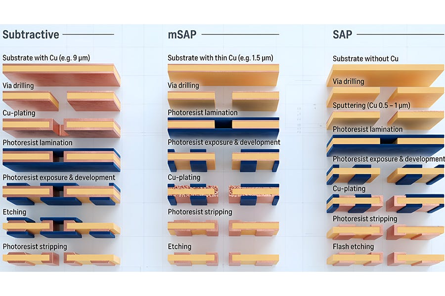
mSAP = modified semi additive process. It is a circuit making process to obtain high quality fine copper traces with more dimensionally accurate than traditional subtractive etching process. In a traditional manufacturing process, circuits are created by etching away thick copper. In mSAP, the process starts with: very thin copper layer, then copper is plated in required circuit areas only and the remaining thin seed copper is dissolved through controlled flash etching. This contrast provides mSAP with powerful line width/space and conductor profile, as well as routing density advantages. HQICSUBSTRATE, a high end mSAP IC Substrate manufacturer can usually provide finer line and space capability than conventional PCB manufacturing, and the technology is applicable to Flip Chip BGA, advanced SiP modules, high speed communication packages and other high end application to semiconductor.
mSAP IC Substrate Manufacturing Flow
The process sequence starts with core processing. Substrate core is for mechanical stability and basic electrical connection. The core material must be of a controlled thickness, be non-warping, have good dimensional stability, and be compatible with the thermal expansion of the material used on each side. A good quality mSAP IC Substrate supplier takes advantages of widely used materials, including high performance epoxy resin system, ABF type build up films or other high performance dielectric materials based on package requirements. After core preparation, drilling is done. Mechanical drilling is available for larger holes through the layers, laser drilling technology has been predominantly used for microvias in build-up layers. It is the time to apply desmear treatment to eliminate resin residues and to augment copper adhesion after the holes are drilled. Bad desmear control can cause void, weak via reliability, or electrical failure. The next step is seed layer formation. A very thin copper film is deposited over the substrate surface and inside holes or vias. This layer of copper allows for electricity flow to the next electroplating step. In mSAP, the thin copper layer is significant as it enables later etching to be very light, which mitigates lateral copper loss and keeps circuit dimensions accurate. Photoresist lamination and exposure on the other hand, are next. Dry film photoresist (DFR) is laminated to the copper under well-defined temperature, pressure and humidity. The circuit pattern is transferred to the resist by direct imaging or by using high resolution exposure systems. The developed photoresist exposes only the areas where copper traces are to be constructed. The advanced mSAP IC Substrate manufacturer must have the capabilities of controlling exposure energy, alignment accuracy, film thickness, and development stability to avoid shorts, opens, and line deformation. Copper pattern plating is then done. Copper grows on the exposed seed layer until the required conductor thickness is reached. Uniform plating is important since it influences trace resistance, impedance control, via reliability, and package coplanarity. A proven mSAP IC Substrate manufacturer achieves a uniform copper thickness over the panel using an optimized technology for plating chemistry, current distribution design, agitation control and process monitoring. After plating the photoresist is removed. The seed copper in non circuit areas is stripped off by way of flash etching. As the seed copper layer is very thin, the etching time is limited in order to minimize the side etching. This is the main reason mSAP can achieve finer and more rectangular traces than the subtractive etching. The build up procedure is completely layer by layer until that you have finished your wanted stack up. And finally solder mask, surface finish, routing, electrical testing, aoi, reliability verification etc.. A experienced mSAP IC Substrate provider needs to be able to exercise tight control from are to final shipment.
Key Process Characteristics of mSAP
The first basic trait of mSAP is fine line capability. This facilitates high density routing for chips with large input and output counts. Fine traces allow more signals to go through limited substrate area and can help to eliminate the need of more layers, which leads to higher cost. The second feature is improved conductor geometry. The difference in formation of copper: copper is predominantly plated and not etched from solid block of copper, the trace sidewalls are much more vertical and the top-to-bottom width variation is much smaller. This leads to enhanced impedance uniformity and high speed signal performance. The third characteristic is enhanced design flexibility. mSAPallows for dense via structures, narrow line pitch, tight routing channels, and highly multilayer solutions. For high end packages, partner with a leading mSAP IC Substrate manufacture to optimize stack up, via design, pad structure and routing rules. Process sensitivity is the fourth attribute. mSAP needs clean rooms, high resolution imaging, precise plating, stable etching, tight registration control. Minimal particles, plating defects, resist residues, or over etching can contribute to yield loss. Hence, process discipline is? fundamental capability for a robust mSAP IC Substrate manufacturer.
Subtractive Process versus mSAP
Subtractive processing is one of the oldest methods for manufacturing circuits. It is made of copper clad laminate. The desired circuit is protected by the photoresist, while the unwanted copper is removed by chemical etching. It’s a proven, robust process that provides high productivity and cost effectiveness at standard line widths. But the subtractive process also has limitations when used for fine line production. Because the original copper foil is thick, the etchant not only moves vertically into the copper but also underneath the copper laterally. It leads to undercut, rougher edges and trapezoid trace profiles. Therefore, is definitely a challenge to obtain very fine line and space patterns at high yield. Compared to subtractive technology, mSAP provides smaller features, tighter dimensional control, and more dependable high density routing. The trade-off is increasing process complexity and equipment stringency. This is the reason why customers frequently go to a professional mSAP IC Substrate supplier for high-end package substrates.
SAP Compared with mSAP
SAP means semi additive process. It begins from — an insulating dielectric surface with no copper foil. A very thin seed layer is deposited by electroless copper or sputtering. Copper is plated in the patterned regions and then the seed layer is removed. SAP has the best potential for fine lines of the three technologies. It can be used for ultra fine line and space patterns for highest level packaging requirements. SAP (semi-additive process) also has higher requirements on surface pretreatment, seed layer adhesion, equipment precision and production environment. It also faces greater challenges in controlling the cost and yield. mSAP lies somewhere between subtractive and SAP. It is far superior to subtractive etching for fine circuits, yet more feasible and scalable than full SAP for a myriad of high volume applications. An expert mSAP IC Substrate provider will assist customers in selecting the appropriate process window based on density, reliability, cost, and volume of production.
Quality Control and Reliability
Quality control of AFP (mSAP)TC production includes AOI, EL testing for open and short, cross sectioning, copper thickness measurement, microvia inspection, warpage inspection, and thermal reliability testing. Defects in plating, such as residual seed copper, plating voids, resist scum, line necking, via cracks and delamination, should be averted. Reliability is particularly critical since IC substrates need to withstand assembly reflow, thermal cycling, moisture ingress, and extended operation. A reliable High Density IC substrate manufacturer assesses copper adhesion, dielectric integrity, via fatigue life, surface finish quality and package level performance.
Future Outlook
The development of mSAP IC substrate technology in the future corresponded to AI computing, chiplet integration, high bandwidth memory, 5G and 6G communication, automotive intelligence, and advanced data center hardware. These require the use of finer lines, lower loss dielectrics, enhanced thermal management, and/ or higher layer counts. With packaging continuing to evolve, the mSAP IC Substrate manufacturer’s role will grow increasingly significant. Best partners also enable design for manufacturability support, material selection guidance, stack up optimization, and early engineering collaboration. To sum up, mSAP offers the best compromise among fines line performance, production efficiency and processability. Select the desired mSAP IC Substrate manufacturer and guidance on how to choose the most suitable one For semiconductor companies, the right mSAP IC Substrate manufacturer can assist in turning their advanced chip designs into dependable, scalable, and high-performance package solutions.
메타데이터
- post_id
- c19bcd6fea27
- slug
- deep-to-learn-msap-ic-substrate-c19bcd6fea27
- url
- https://medium.com/@wyg28291/deep-to-learn-msap-ic-substrate-c19bcd6fea27
- canonical_url
- https://medium.com/@wyg28291/deep-to-learn-msap-ic-substrate-c19bcd6fea27
- author_url
- https://medium.com/@wyg28291
- status
- ok
- fetched_at
- 2026-07-11 06:06:52