Who Needs AI Chips When You Can Have an AI Wafer?
Cerebras’s day-one doubling was not a story about the IPO. It was a story about a physical constraint on inference, and about what the…
Who Needs AI Chips When You Can Have an AI Wafer?
Cerebras’s day-one doubling was not a story about the IPO. It was a story about a physical constraint on inference, and about what the company’s commercial traction reveals about where AI workloads are heading.
Cerebras Systems went public on Nasdaq this morning under the ticker CBRS, pricing at $185 per share, opening at $350, briefly trading as high as $385, and settling near $330 by mid-afternoon, raising $5.55 billion on a fully diluted valuation above $100 billion.
Cerebras IPO: The largest U.S. technology IPO since Uber’s 2019 debut.
Cerebras filed its original S-1 in September 2024, withdrew it after intense regulatory scrutiny over customer concentration in the UAE, refiled, watched its indicated range climb from $115–125 to $150–160 to a final price of $185, and spent the intervening eighteen months repositioning from a hardware systems vendor into an inference cloud provider. None of that biographical context explains why the stock doubled on day one. What explains it is physics.
Cerebras was founded on a single technical premise: the constraint on neural network inference is not transistor count, not die area, and not the sophistication of the compiler stack. It is the time required to move weight parameters from wherever they are stored into the arithmetic units that need them. Every GPU cluster ever built (Hopper, Blackwell, MI300X, GB300) runs autoregressive token generation at 3–8% of its rated compute utilization, not because the arithmetic units are slow but because the memory hierarchy cannot feed them fast enough. Cerebras’s answer was to eliminate the hierarchy entirely by making the chip as large as the wafer it was printed on.
The Roofline Problem: Why Decode Runs at a Fraction of Rated Compute
The physics constraint that Cerebras identified in 2016 has a precise name in computer architecture: arithmetic intensity, measured in floating-point operations per byte of memory traffic. A GPU’s roofline model has two regimes: compute-bound operations where the arithmetic units are the bottleneck, and memory-bandwidth-bound operations where data movement is the bottleneck.
Training a large model at high batch size is compute-bound: each weight byte loaded from HBM is used hundreds of times across the batch before being evicted, so arithmetic intensity is high and the GPU’s tensor cores are well-utilized.
Autoregressive inference decode at batch size 1 is the opposite extreme: each weight parameter must be loaded from HBM to generate a single token, used once for a single multiply-accumulate operation, and then reloaded for the next token.
Arithmetic intensity collapses to roughly 1 FLOP per byte. An H100 SXM with 3.35 TB/s of HBM3e bandwidth delivers a theoretical ceiling of approximately 3.35 teraFLOPS under this access pattern — against a rated 989 teraFLOPS of FP16 dense compute. The GPU is sitting at 0.3% of rated throughput, throttled entirely by the speed at which HBM can deliver weight bytes to the tensor cores. Stacking more HBM or widening the NVLink fabric does not change this regime; it shifts the ceiling by a constant factor while the access pattern remains the binding constraint. The only way to escape it is to move the weights closer to the arithmetic units — physically, not logically. That is what wafer-scale integration does.

Figure 1 — Roofline model showing H100 and WSE-3 ceilings. At the arithmetic intensity of autoregressive decode (AI ≈ 1 FLOP/byte), WSE-3’s 21 PB/s on-chip SRAM bandwidth enables roughly 6,000× the effective throughput of H100’s 3.35 TB/s HBM3e. Training at high batch size sits in the compute-bound regime where H100’s dense FLOP count advantages re-emerge. The two architectures are optimized for different points on the same curve.
WSE-1: Making the Wafer Manufacturable
The WSE-1, introduced in 2019 on TSMC 16nm, was the proof of concept that the wafer-scale proposition was manufacturable. At 46,225 mm² it is still, by a wide margin, the largest integrated circuit ever built — roughly 57 times the area of a reticle-limited die. It integrated 1.2 trillion transistors, 400,000 AI-optimized cores, and 18 GB of on-chip SRAM delivering 9 PB/s of fabric bandwidth. The engineering problem that should have killed the project was yield.
Semiconductor manufacturing introduces random defects at rates that scale with die area: a 46,000 mm² wafer accumulates hundreds of potential defect sites that would, on a conventional product, mean discarding the entire unit. Cerebras solved this with a proprietary defect-tolerant routing fabric built into the design, a mesh interconnect with redundant pathways allowing any failed core to be bypassed transparently, so a wafer with dozens of dead cores still ships as a functional product.
The physical execution required an equally unconventional manufacturing decision: the scribe lines (the keep-out zones normally reserved for dicing a wafer into individual dies) were repurposed as wiring channels for the on-wafer data fabric that connects all 84 die steppings into a single coherent compute domain. What the semiconductor industry treats as wasted space, Cerebras turned into interconnect.
WSE-2 and WSE-3: Scaling Up, and a Specification Worth Reading Closely
The WSE-2 (2021, TSMC 7nm) doubled the scale: 2.6 trillion transistors, 850,000 cores, 40 GB of on-chip SRAM, 20 PB/s of fabric bandwidth. The CS-2 system that housed it became Cerebras’s first production commercial product. WSE-3 followed in 2023 on TSMC N5, reaching 4 trillion transistors and 970,000 total cores, of which 900,000 are enabled, with the remaining 70,000 held as redundancy for yield harvesting. On-chip SRAM expanded to 44 GB at 21 PB/s.
The manufacturing process evolved with it: each production batch of WSE-3 wafers requires a custom mask set for the upper metal layers, individually generated to route around the specific defect pattern of that batch. This is an unusual and materially expensive step. Standard semiconductor production uses the same mask set across all wafers in a product lifetime; Cerebras recuts per-batch because intra-batch process variation is substantially lower than cross-batch variation, meaning a mask optimized for one batch’s defect topology does not transfer reliably to the next.
The result is near-100% usable yield from TSMC output, which is necessary economics at the volume Cerebras now needs to honor its OpenAI supply commitment. One specification requires care in reading: Cerebras’s published 125 PFLOPs for WSE-3 assumes 8:1 unstructured sparsity. Dense FP16 throughput is 15.6 PFLOPs — still a substantial number, but roughly one-eighth the headline. SemiAnalysis has termed this “Feldman’s Formula,” and it is a reminder that accelerator marketing specs require the same denominator-checking discipline that applies to every vendor in the space.

Figure 2 — WSE generation progression. Die area is constant across all three generations — 46,225 mm², full wafer — while process node improvements drive transistor density, core count, and SRAM capacity. On-chip SRAM and fabric bandwidth are merged into a single row for clarity. Off-wafer I/O (red) is the persistent structural constraint: the physical perimeter of the wafer limits SerDes placement regardless of process node.
Off-Wafer Bandwidth: Where the GPU Comparison Breaks Down
The constraint highlighted in red in Figure 2 (150 GB/s of off-wafer I/O bandwidth) is not an oversight in the WSE-3 design. It is a consequence of geometry. A conventional GPU die has perimeter-to-area ratios that leave room for hundreds of SerDes lanes at the die edge. A wafer-scale chip has 57 times the area but only roughly 7.5 times the linear perimeter, and that perimeter must also carry power, ground, and control signals.
The available edge bandwidth per unit of silicon area is structurally lower on a wafer-scale device. This is where the comparison to NVIDIA and AMD becomes sharpest, and where understanding what each architecture is actually designed to do prevents false equivalence. NVIDIA’s scale-up strategy in NVL72 provides 1.8 TB/s of NVLink 6 bandwidth per GPU, with 72 GPUs interconnected through NVSwitch at 260 TB/s of aggregate all-to-all bandwidth. Every GPU sees every other GPU at full bandwidth, no traversal penalty, no routing overhead.
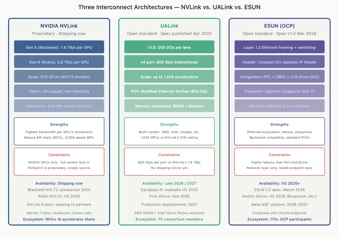
AMD’s Helios targets the same 72-GPU domain and the same 260 TB/s aggregate through UALink, the open-standard fabric we documented in our analysis of the interconnect wars. Both architectures treat scale-out networking as a first-class design objective — the cluster is the compute unit, and the interconnect is what makes it behave as one.
Cerebras’s SwarmX fabric connects up to 192 CS-3 systems, but at 150 GB/s off-wafer I/O per system, each wafer communicates with its neighbors at roughly 8% of what an H100 NVLink lane provides. That number is not in the same category. The two architectures are not competing on the same axis.

Figure 3 — Scale-up topology comparison. NVIDIA NVL72 and AMD Helios both target ~260 TB/s aggregate all-to-all bandwidth for 72-GPU coherent compute domains. Cerebras SwarmX connects up to 192 CS-3 units at 150 GB/s per inter-unit link — 12× lower than a single GPU’s NVLink lane. The design philosophies diverge accordingly: GPU clusters shard one large model across many accelerators; Cerebras runs independent inference streams, each served by a self-contained wafer.
Where the CS-3 Actually Competes: Sub-70B Models at Low Batch Size
This architectural divergence resolves into a competitive positioning that is more complementary than it first appears. Because the WSE-3 cannot efficiently shard a single large model across multiple wafers at GPU-cluster communication rates, it is not the right tool for serving a 400B+ parameter model as a unified inference backend.
A single CS-3 with MemoryX can hold approximately 70B parameters in FP8 entirely in SRAM — exactly the model class (Llama 3 70B, Qwen 72B, Mistral 70B) that dominates enterprise and API inference workloads by request volume. Models larger than the 44 GB SRAM capacity spill into MemoryX DRAM, which introduces off-chip memory latency for a portion of weight reads and partially erodes the bandwidth advantage that makes the wafer compelling. The CS-3’s absolute domain is sub-70B models served at low batch size and maximum interactivity — precisely the regime where GPU-based inference is most inefficient.
Cerebras publishes benchmarks showing 450,000 tokens per second on Llama 2 70B on a single CS-3, against roughly 10,000–15,000 tokens per second on a single H100. SemiAnalysis’s InferenceX benchmark frames this as the throughput-interactivity frontier: a GPU cluster is a bus, optimized to carry maximum aggregate payload at moderate per-passenger speed; the WSE-3 is a different vehicle entirely, one that delivers individual users thousands of tokens per second at speeds that GPU serving cannot reach at any batch size configuration. The two vehicles serve different traffic patterns.
The CS-3’s customer, at the end of 2026, is not the infrastructure team asking “what is my maximum aggregate throughput?” but the application team asking “how do I make this latency-critical pipeline feel instant?”
The Agentic Loop: How Latency Became a Commercial Variable
That second question has become commercially significant in a way it was not eighteen months ago. The agentic-loop architecture, where a single user action triggers ten, twenty, or fifty sequential model calls, each conditioned on the output of the prior, serializes latency in a way that batch throughput cannot hide.
- A tool-calling agent that invokes an LLM fifty times per user request, with each call generating 500 tokens, accumulates 25,000 tokens of serial decode work.
- On a well-loaded H100 serving at 50 tokens per second per user under moderate concurrency, that chain introduces 500 seconds of wall-clock latency — plainly unusable as an interactive application.
- On a CS-3 serving at 2,000 tokens per second per user, the identical chain completes in 12.5 seconds.
- At higher CS-3 speeds under favorable conditions, it collapses further.
SemiAnalysis identifies this inflection, the point at which agentic coding workflows made token generation speed the primary UX bottleneck rather than model capability, as the moment the market repriced SRAM-machine architectures entirely.
The data point that anchors the commercial argument: Anthropic’s fast-mode tier charges a 6× price premium for approximately 2.5× the interactivity of standard mode. Users paid it.
Eighty percent of SemiAnalysis’s own AI spend at peak was on that fast-mode tier, and its engineers refused to migrate to a newer model that lacked the speed tier. Past a capability threshold, revealed preference runs toward speed, and the price elasticity curve for low-latency tokens is far shallower than the general token market assumed.

Figure 4 — Wall-clock latency accumulation for a 50-step agentic tool-calling chain generating 500 tokens per call. H100 at 50 tokens/second/user accumulates 500 seconds of serial inference latency. GB300 NVL72 at 200 tokens/second reduces this to 125 seconds. CS-3 at roughly 2,000 tokens/second completes the identical chain in approximately 12.5 seconds. The 60-second dashed threshold approximates where agentic workflows transition from a tolerable pipeline to an interactive experience.
The Business Model Pivot: From Hardware Systems to Inference Cloud
The commercial validation of that latency thesis is now written into Cerebras’s revenue structure. OpenAI committed to a 750 MW compute deal, the largest single inference infrastructure contract publicly disclosed, that will require Cerebras to ship more CS-3 systems by 2028 than it has shipped across its entire history.
OpenAI launched its first production model running on Cerebras hardware earlier this year. AWS followed with a formal partnership. The customer list also includes G42, which was both the company’s commercial lifeline and its regulatory liability during the aborted 2024 IPO: the original S-1 disclosed that G42 represented the majority of revenue, drawing CFIUS scrutiny that forced the filing withdrawal. Cerebras resolved the concentration risk not by finding new customers — though it did that — but by pivoting its business model. Hardware systems sales produce lumpy, capital-intensive revenue tied to specific datacenter build-outs. Inference cloud services produce recurring, predictable revenue tied to API consumption.
The business that went public today is primarily an inference cloud, with the hardware as the proprietary infrastructure advantage that makes its latency profile impossible to replicate on commodity GPU clusters. That positioning is the same story that NVIDIA wrote with DGX Cloud and that AMD is attempting with its own cloud inference offerings, but Cerebras has a defensible technical moat in its performance regime that neither incumbent can replicate by stacking more HBM or widening an NVLink fabric.

Figure 5 — CS-3 system architecture. The WSE-3 wafer occupies the chassis center with a custom Vicor engine block for power delivery and liquid cooling alongside it. The I/O block provides 150 GB/s of off-wafer bandwidth — the structural ceiling imposed by wafer-edge geometry. External MemoryX expands weight capacity to 1.5 TB via off-chip DRAM; SwarmX connects up to 192 CS-3 units for parallel inference stream scale-out.
WSE-4: What the Next Generation Might Resolve, and What It Will Not
The forward trajectory carries one announced product and several unresolved questions. WSE-4 is in development on TSMC 3nm, with additional SRAM capacity expected (industry estimates in the 60–80 GB range) and continued fabric bandwidth improvements. SemiAnalysis reports that Cerebras is pursuing hybrid-bonded wafer-scale optical transceivers, an engineering effort the company frames as primarily targeting HPC workloads rather than LLM inference.
The more pressing architectural question for WSE-4 is whether expanded on-chip SRAM can address the 70B–400B model range more competitively as frontier model sizes continue growing — a WSE-4 with 80 GB of SRAM could hold a 70B FP8 model entirely on-chip with headroom for KV cache, eliminating the MemoryX latency penalty for the most commercially active model class. Whether that is achievable within the thermal constraints of a 3nm wafer at 46,225 mm² is the central question Cerebras has not yet disclosed.
The off-wafer bandwidth constraint remains structurally unchanged by process node transitions: unless WSE-4 introduces a new I/O architecture, the 150 GB/s ceiling will continue to define the upper boundary of model sizes that can be served efficiently from a single wafer, and the lower boundary of the model sizes that require MemoryX to serve at all.
The Larger Signal: An Industry Outgrowing a Single Hardware Abstraction
The more useful lens for placing Cerebras in the infrastructure landscape is not whether wafer-scale silicon is better than GPUs, but rather what the CS-3’s commercial traction reveals about where AI workloads are heading. The GPU has dominated AI infrastructure because of its generality: a single H100 can train, do batch inference, run small models, run large models, handle prefill, and handle decode — all with the same hardware at varying efficiency. That generality is enormously valuable when workload profiles are uncertain, as they were in 2020 and 2021.
What Cerebras’s IPO and OpenAI’s 750 MW commitment suggest is that at least one significant category of workload — low-batch, latency-critical, interactive and agentic inference at the 7B–70B model range — has become predictable enough and commercially large enough to justify purpose-built silicon. The same fragmentation logic already appeared with Groq’s LPU (subsequently acquired by NVIDIA for $20 billion), with Google’s TPU, and with the disaggregated prefill/decode serving architectures we documented in our analysis of the inference stack.
In each case, a workload that once ran acceptably on general-purpose GPU hardware became large enough to attract purpose-optimized design. This is not a story about one architecture defeating another. It is a story about an industry maturing past the point where a single hardware abstraction can efficiently serve every workload class simultaneously.
The GPU remains the most versatile and highest-volume platform in AI infrastructure, and that position is unlikely to change. What is changing is the set of workloads for which the GPU is the only credible answer, and that set is narrowing as specific use cases become large enough to support dedicated alternatives. Cerebras is one such alternative, with a clearly defined performance regime, real structural limitations, and a commercial trajectory that now carries the additional scrutiny of quarterly public earnings. How that scrutiny resolves will say as much about the economics of workload-matched silicon as it will about Cerebras specifically.
Sources: SemiAnalysis, “Cerebras — Faster Tokens Please”, Myron Xie, Jordan Nanos, Max Kan et al., May 13, 2026 • CNBC, “Cerebras prices IPO above expected range”, May 13, 2026 • CNBC, “Cerebras almost doubles in Nasdaq debut, topping $100 billion market cap”, May 14, 2026 • TechCrunch, “Cerebras raises $5.5B, then stock pops 108%, in the first huge tech IPO of 2026”, Julie Bort, May 14, 2026 • Bloomberg/Reuters, CBRS IPO pricing and trading data, May 14, 2026 • Cerebras Systems, Hot Chips 35, “WSE-3: The Third Generation Wafer Scale Engine”, 2023 • SemiAnalysis InferenceX Dashboard, May 2026 • SemiAnalysis, “Cerebras Wafer-Scale Hardware Crushes”, Dylan Patel, June 2021
메타데이터
- post_id
- c778da074945
- slug
- who-needs-ai-chips-when-you-can-have-an-ai-wafer-c778da074945
- url
- https://medium.com/teradata-labs/who-needs-ai-chips-when-you-can-have-an-ai-wafer-c778da074945
- canonical_url
- https://medium.com/teradata-labs/who-needs-ai-chips-when-you-can-have-an-ai-wafer-c778da074945
- author_url
- https://medium.com/@brandon.mincey_1754
- status
- ok
- fetched_at
- 2026-06-09 15:37:30