Computer Memory Part V: Volatile Memory
We discuss volatile memory including DRAM, SRAM, and registers.
Computer Memory Part V: Volatile Memory
This post does not reflect the views of current, past, or future employers. The opinions in this article are my own.
In the past couple of articles we looked at [non-volatile memory](http://SRAM using flip-flops rather than capacitors to store a bit of data. A flip-flop is a fundamental digital electronics circuit used to store one bit of binary data (i.e. a 0 or a 1). A flip-flop is bistable meaning it has two stable states and can "flip" or "flop" between them, triggered by a clock signal. These transistors of an SRAM are arranged as two cross-coupled inverters, providing a "static" feedback loop that holds the value until it is actively overwritten. The feedback loop means that current is continuously flowing hence SRAM requires more power consumption than DRAM. Reading and writing an SRAM cell An SRAM cell is read by reading the voltage difference of the two sides of the cell. This indicates the current state of the flip-flop as holding a 0 bit or 1 bit. Reading a bit is nondestructive. A write operation is performed by activating the work line and bit limes to set the flip-flop to the desired state. Similar to DRAM, SRAM is organized into a two dimensional array that allows bits of a word to be read or written in parallel. SRAM tail of the tape Technology: Flip-flops in semiconductos Memory capacity: Afew kilobytes (KB) to about 16 megabytes (MB) per chip. Access time: Less than 10 nanoseconds. Advantages: Static Random Access Memory (SRAM) offers superior speed, lower access time, and higher reliability compared to DRAM because it does not require periodic refreshing to maintain data. Disadvantages: Compared to DRAM, SRAM has higher cost, lower memory density, and generates significant heat. Register memory Register memory is the highest performance memmory in a computer. Registers a integrated in the CPU and are synchronized by a clock signal, loading new data only during clock pulses while maintaining state at other times. Registers are super fast with access times of one clock cycle (e.g. around 300 picosends on a 3GHz CPU. How does register memory work Similar to SRAM, a cell in a register memory is constructed from flip-flops. Because registers are directly wired into the CPU to allow simulateneous access of different registers there is more wiring need than SRAM hence register cells are physically larger then SRAM cells. Register memory tail of the tape Technology: Flip-flops in semiconductos Memory capacity: A few hundred kilobits. For instance, the register file for 64-bit a RISC-V CPU has thirty-two sixty-four bit registers for 2048 bit (plus a few hidden registers). Access time: 300 to 500 picoseconds (0.3 to 0.5 nanoseconds) Advantages: The fastest memory in a computer used as input and output operands of CPU instructions. Disadvantages: Very limited capacity and high cost.), so today we’re covering volatile memory. The easiest way to think about it is that non-volatile memory continues to store data even when your computer is powered off, but with volatile memory the second you flip your computer off all the data goes away. So volatile memory isn’t suitable for data storage, but is instead used as temporary memory during computation, that is as a program runs it uses volatile memory to hold intermediate results that are needed for a few seconds or maybe even just a few microseconds.
Because volatile memory is used in computation it has to be fast! In a modern computer we expect access times in order of tens of nanoseconds for DRAM access down to single digit access times for registers. It’s this stringent requirements on access time that justifies the need to volatile memory since all of the non-volatile memory types we talked about have much higher access times.
A bit of history
As we talked about previously, the first computer memory used in the computation path was magnetic drum memory. That was replaced by magnetic core memory. This was transitioning from non-volatile memory with moving parts to non-volatile memory without moving parts. The access time improvement is stark: over ten milliseconds for magnetic drum memory compared to less than ten microseconds for magnetic core memory. Interestingly both of these were non-volatile, which even today might have advantages in dealing with power interruptions.
Magnetic core memory was hugely revolutionary, but had low memory density and high manufacturing costs. The answer to overcome the limitations was semiconductors!
The rise of DRAM
In 1968, Robert Dennard at IBM patented Dynamic Random Access Memory (DRAM), which used a single transistor and a capacitor to store a bit. The structure enables millions, now billions, of cells to be packed onto a single small chip resulting in much higher memory densities than core memory could ever dream of.
In 1970 Intel released the first first commercially available DRAM chip, the Intel 1103, which began to replace core memory. The 1103 had a whopping one kilobit capacity and 500 nanoseconds access time. It took a couple of spins to get it right, but once it was out magnetic core memory was quickly replaced.
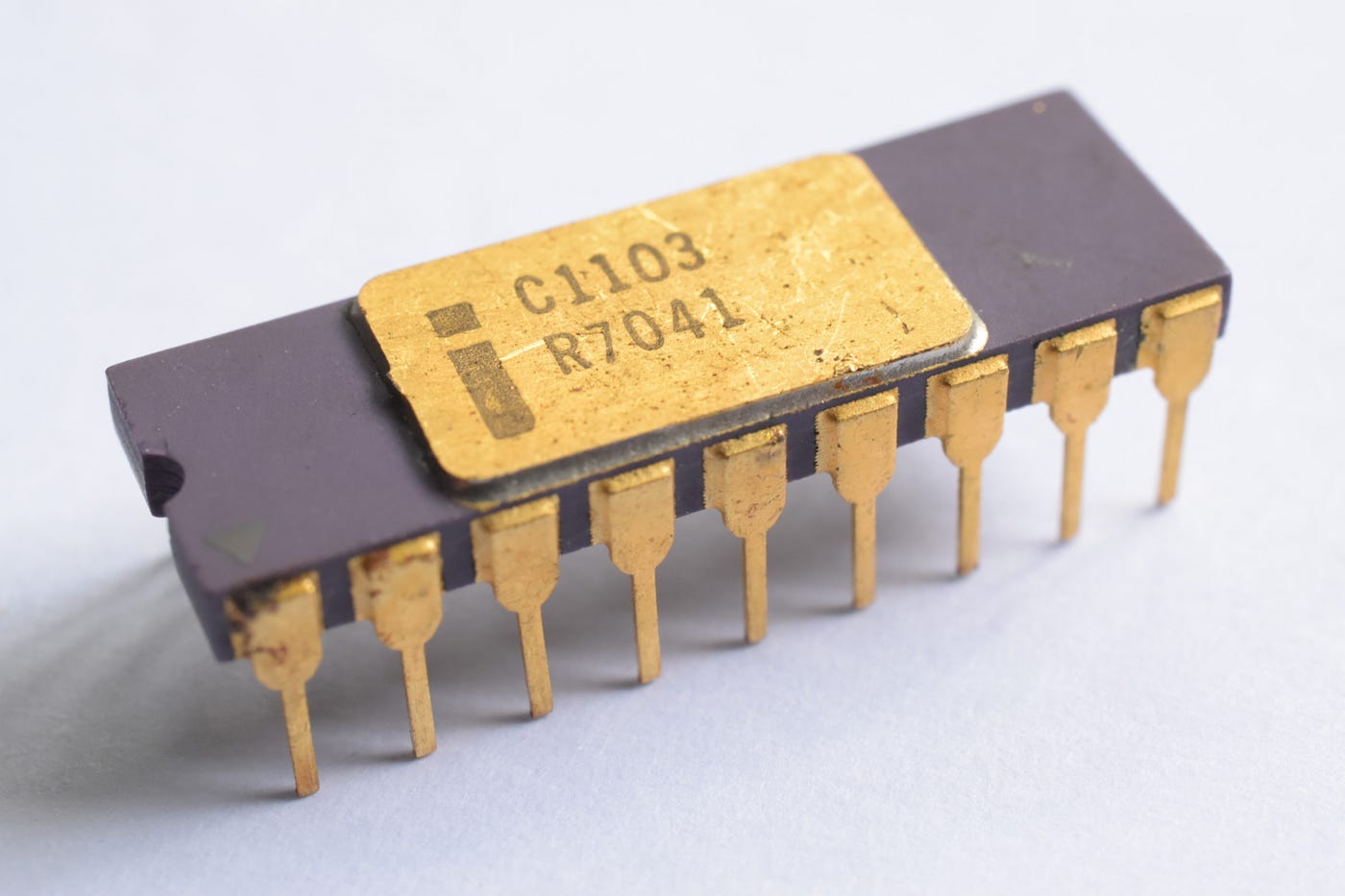
The Intel 1103 package.
DRAM and PCs
In the eighties, DRAM continued to improve in both density and access time. Chips moved from to 4 kilobytes, to 16 kilobytes, to 64 kilobytes. As CPU speeds increased, memory evolved to reduce access time and increase bandwidth. DRAM moved to SDRAM (Synchronous DRAM) and later to DDR (Double Data Rate) SDRAM. The evolution of CPUs and DRAM is really what drove the PC revolution of the eighties!
Today’s DRAM
Memory in a modern computer is usually in the form of **DIMMs (Dual In-line Memory M**odules) generally contain 8GB, 16GB, or 32GB of DRAM per stick for consumer desktops, while modern DDR5 workstation and server modules can reach 64GB, 128GB, or even 256GB per stick. High end servers, like those used in AI, can have of 24 Terabytes of memory — and some have up to 40 Terabytes.

Hynix Hmcg94mebra Memory 64GB DDR5 4800MHz DIMM. The black chips on the circuit board contain DRAM memory. The DIMM is inserted in a DIMM slot on a computer motherboard.
DRAM
DRAM is the most common in a modern computer. DRAM stands for Dynamic Random Access Memory. The “Random Access Memory” part, i.e. RAM, allows the CPU to read/write data at any address directly (randomly) rather than sequentially like we might do in a Hard Disk Drive. DRAM is “Dynamic” because it requires periodic electrical refreshing to maintain data. It stores each bit in a capacitor that naturally leaks charge over time. To prevent data loss, the memory controller must recharge these capacitors every few milliseconds.
How does DRAM work?
A DRAM memory cell is composed of a transistor and a capacitor. The value held in the memory cell depends on whether the capacitor is charged. If the capacitor is charged then the cell holds a ‘1’ bit, else if the capacitor is not charged then the cell holds a ‘0’ bit.
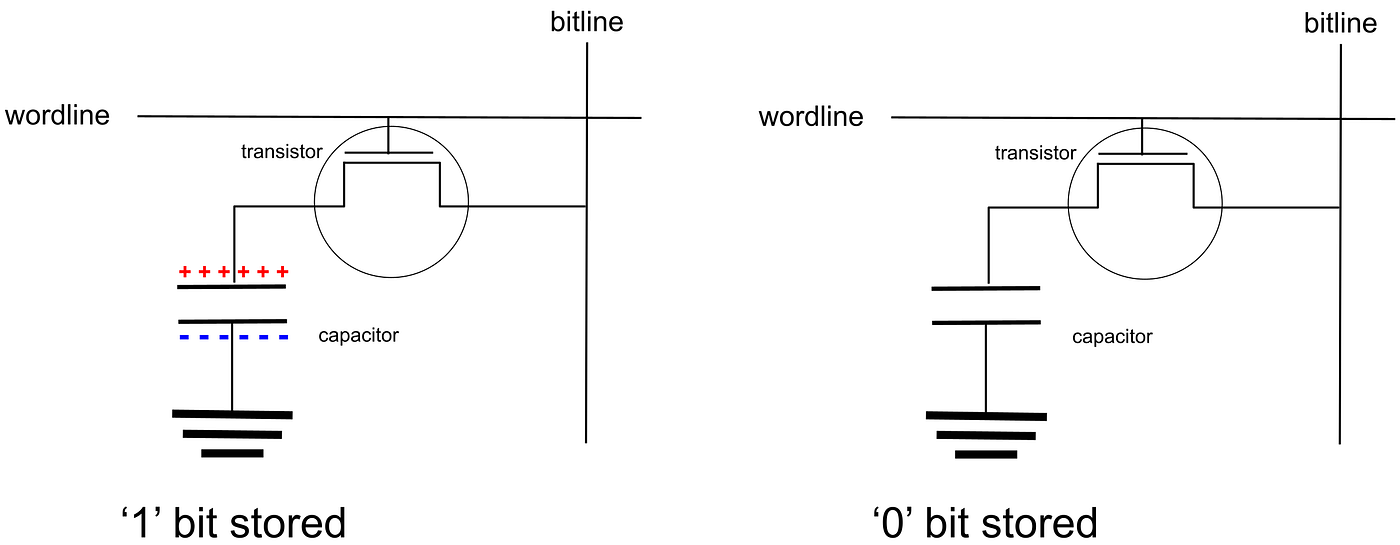
DRAM memory cells. Each cell is made up of a capacitor and a transistor. The capacitor can be charged to signify a 1 bit (shown in the cell on the left) or uncharged to signify a 0 bit (cell on the right). The transistor is opened to read or write the bit.
A DRAM chip is organized as a two dimensional array of cells. Each row of cells is one word (e.g. 8 bits for a byte) and a row is selected by driving a word line high. The cells in a column are connected by a bit line that is used to read or write the bit selected by the word line. The emitter of each transistor is connected to the capacitor, the collector is connected to a bit line, and the gate is connected to a word line.

Example DRAM containing four 4-bit words. A read operation for word #1 is in progress. The wordline for word #1 is activated causing the cells in the row to discharge the capacitor in their bit line. A sense amplifier connected to each bitline detects the bitline voltage and interprets it as reading a 0 bit or 1 bit. A value of 0b01010 is returned on the data bus as the result of the read in this example.
Reading a bit
The word line for the desired word (i.e. row) is driven to a high voltage. This opens the transistor allowing current to flow from the capacitor over the bit line. If the capacitor is charged (signifying a 1 bit), charge flows out, slightly raising the bitline voltage, otherwise if it is empty (signifying a 0 bit), charge flows in, slightly lowering the bitline voltage. A sense amplifier detects the small voltage difference, amplifying it to the full rail voltage (0 or 1) which is then conveyed over a data bus. This happens for each of the memory cells in a word so that each line of the data bus is set to a 0 or 1 value that was read.
Reading a memory cell is destructive, that is it destroys the data held in the capacitor, so the sense amplifier immediately writes the data back into the cell.
Writing a bit
The word line for the desired word (i.e. row) is driven to a high voltage. The bit line is set to a high or low voltage by the sense amplifier. If the voltage is high then the capacitor is charged (a 1 bit is set), otherwise the capacitor is discharged (a 0 bit is set). This happens for each of the memory cells in a word so that the value of each line of the data base sets a 0 or 1 in the appropriate memory cell.
Refresh
DRAM is dynamic, meaning it requires constant refreshing. The capacitors in the memory cells gradually lose their charge, so they need to be recharged every few milliseconds to prevent data loss. This is done by reading the memory cell and writing it back immediately. DRAM interacts with other circuits to manage the identification of rows and columns, oversee the refresh process, and instruct whether to accept a charge. These circuits also facilitate reading and restoring data efficiently.
Types of DRAM
There are various types of DRAM that offer different tradeoffs and characteristics in performance and cost.
- SDRAM (Synchronous DRAM): Synchronizes with the CPU clock to process data faster than older asynchronous types.
- DDR SDRAM (Double Data Rate): Transfers data on both the rising and falling edges of the clock signal, hence doubling bandwidth.
- DDR1, DDR2, DDR3, DDR4, DDR5: Successive generations offering higher speeds, lower power consumption, and better performance.
- LPDDR (Low Power DDR): Optimized for lower power consumption in mobile phones, laptops, and tablets.
- GDDR (Graphics DDR): Specialized memory designed for graphics cards and high-performance, bandwidth-intensive tasks.
- RDRAM (Rambus DRAM): An older technology that was popular in the early 2000s for, among other things, graphics cards.
- Asynchronous DRAM: An obsolete type that did not synchronize with the CPU clock, used in early PCs.
- High Bandwidth Memory (HBM): A high-speed, 3D-stacked DRAM technology designed for data-intensive applications like AI, GPUs, and high-performance computing.
The most popular DRAM types today are DDR4 and DDR5. DDR5 offers faster speeds (starting at 4800+ MHz vs. 3200 MHz), higher capacities (up to 64GB+ per stick), and better power efficiency (1.1V vs. 1.2V) compared to DDR4, but requires a modern CPU and motherboard. While DDR5 provides better performance, DDR4 remains cost-effective for budget systems.
DRAM tail of the tape
Technology: Dynamic memory cells composed of a transistor and a capacitor.
Memory capacity: Current DRAM chips often reach 16 Gb or 32 Gb per die, enabling high-capacity DDR5 sticks, while mobile DRAM commonly uses 4 GB to 12 GB+ capacities.
Access time: 10 to 60 nanoseconds.
Advantages: The simple design of a DRAM cell allows high density, low cost per bit, fast access time, and lower power consumption than SRAM.
Disadvantages: The primary disadvantage of DRAM is that it requires memory cells to be periodically refreshed, the result is that DRAM has higher access times than SRAM.
SRAM
Static Random Access Memory (SRAM) is a type of fast, volatile memory that avoids the need for refreshes to retain data — hence the “Static” in SRAM. This allows for lower access times than DRAM so it’s ideal to serve as CPU cache memory (e.g. L1, L2, or L3 caches). An SRAM cell is composed of four to six transistors and doesn’t employ a capacitor. The tradeoff for lower access time is that SRAM has a lower memory density, higher power consumption, and higher cost than DRAM.
How does SRAM work?
SRAM uses flip-flops rather than capacitors to store a bit of data. A flip-flop is a fundamental digital electronics circuit used to store one bit of binary data (i.e. a 0 or a 1). A flip-flop is bistable, meaning it has two stable states and can “flip” or “flop” between them, triggered by a clock signal. These transistors of an SRAM are arranged as two cross-coupled inverters, providing a “static” feedback loop that holds the value until it is actively overwritten. The feedback loop means that current is continuously flowing hence SRAM requires more power consumption than DRAM.

A four transistor SRAM memory cell.
Reading and writing an SRAM cell
An SRAM cell is read by reading the voltage difference of the two sides of the cell. This indicates the current state of the flip-flop as holding a 0 bit or 1 bit. Reading a bit is nondestructive.
A write operation is performed by activating the work line and bit lines to set the flip-flop to the desired state.
Similar to DRAM, SRAM is organized into a two dimensional array that allows bits of a word to be read or written in parallel.

Image of a CPU die show L1, L2, and L3 caches.
SRAM tail of the tape
Technology: Flip-flops in semiconductors,
Memory capacity: A few kilobytes (KB) to about 16 megabytes (MB) per chip.
Access time: Less than 10 nanoseconds.
Advantages: Static Random Access Memory (SRAM) offers superior speed, lower access time, and higher reliability compared to DRAM because it does not require periodic refreshing to maintain data.
Disadvantages: Compared to DRAM, SRAM has higher cost, lower memory density, higher power consumption, and generates significant heat.
Register memory
Register memory is the highest performance memory in a computer. Registers are integrated in the CPU and are synchronized by a clock signal, loading new data only during clock pulses while maintaining state at other times. Registers are super fast with access times of one clock cycle (e.g. around 300 picosends on a 3GHz CPU).

Registers in a CPU. This shows an 8080A CPU that had seven 8-bit registers. Note the proximity of the registers to the Arithmetic Logic Unit (ALU) to minimize latency. The usual goal is that registers are accessed in one CPU clock cycle. When an instruction is executed, registers are accessed in the Instruction Fetch stage (IF), Decode stage (ID), Write Back stage (WB). In other words performance of a CPU is directly correlated to performance of accessing registers (there’s a lot more to this story!).
How does register memory work
Similar to SRAM, a cell in a register memory is constructed from flip-flops. Because registers are directly wired into the CPU to allow simultaneous access of different registers there is more wiring need than SRAM hence register cells are physically larger than SRAM cells.
Register memory tail of the tape
Technology: Flip-flops in semiconductors.
Memory capacity: A few hundred kilobits. For instance, the register file for a 64-bit RISC-V CPU has thirty-two sixty-four bit registers for 2048 bit (plus a few hidden registers).
Access time: 300 to 500 picoseconds (0.3 to 0.5 nanoseconds)
Advantages: The fastest memory in a computer used as input and output operands of CPU instructions.
Disadvantages: Very limited capacity and high cost.
메타데이터
- post_id
- d2ac7b411203
- slug
- computer-memory-part-v-volatile-memory-d2ac7b411203
- url
- https://medium.com/@tom_84912/computer-memory-part-v-volatile-memory-d2ac7b411203
- canonical_url
- https://medium.com/@tom_84912/computer-memory-part-v-volatile-memory-d2ac7b411203
- author_url
- https://medium.com/@tom_84912
- status
- ok
- fetched_at
- 2026-06-15 20:49:13