Our first 24-hour Analog Electronics Competition!
As the professional scroller/ procrastinator I am, I was scrolling through WhatsApp until I came across this post. It read “Test your…
Our first 24-hour Analog Electronics Competition!
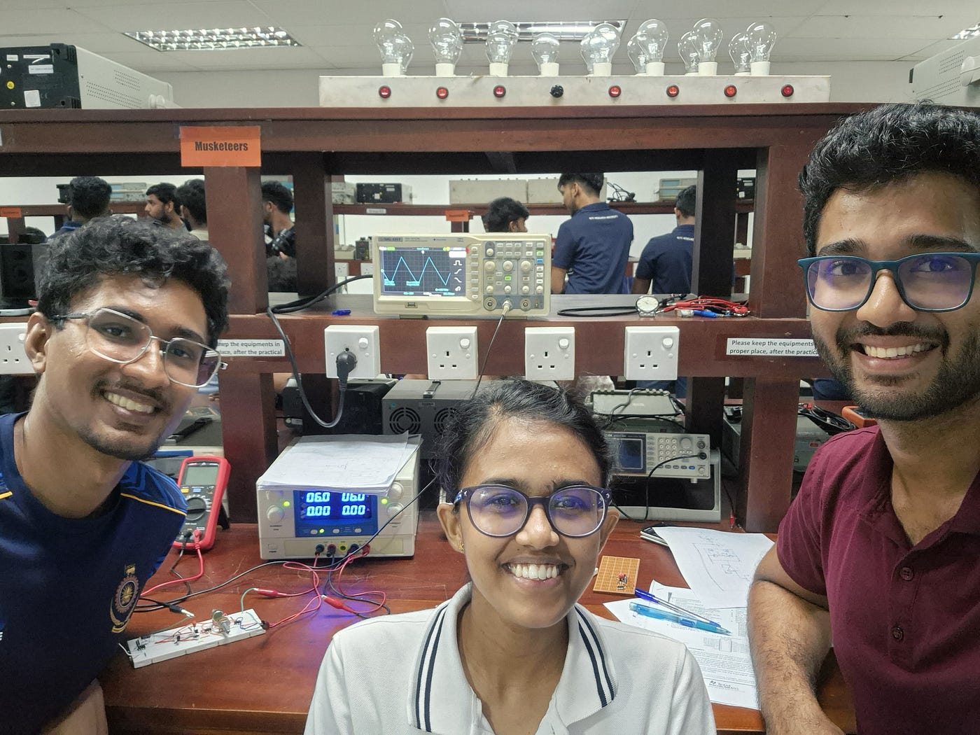
Team Musketeers
As the professional scroller/ procrastinator I am, I was scrolling through WhatsApp until I came across this post. It read “Test your creativity and expertise in a 24-hour Analog Electronics Design Competition”. Jaw-dropped I was definitely not missing out on this. It’s not every day you come across an analog-electronics design competition, let alone a 24-hour one. A couple of weeks later, I and my team — Nilakna & Kavishka — were in a Zoom meeting anxiously waiting for the selection test to begin. The selection test was fairly straightforward; we aced through it and waited impatiently for the Design Competition date.
The competition day finally arrived, and we were there — at SLTC Research University in Padukka. We were there early — in fact, a couple of hours early. Our initial impression was that the campus was beautiful and huge. Half an hour later, we realized it was not to be. The campus was pretty small, and we walked through the entire premises in about an hour. Lesson 1: Do not judge a book by it’s cover

At SLTC Research University in Padukka
The time for the competition finally arrived and we waited impatiently waiting for things to unfold. Prof. Nihal introduced us to the competition. We were tasked with building a function generator, using a very fundamental approach. More specifically we had to build a function generator capable of producing triangular waves with each team getting their specifications. Our output triangular wave should be in the frequency range of 12–14 kHz, with an input voltage of 12 V, a rising edge-to-falling edge ratio of 0.8, and an alternating peak-to-peak voltage of 6V. The catch was that no internet was allowed. In fact, phones & laptops were not allowed. Simulations were also out of the picture. It was just three brains working together.
What our team loved about the introduction session was the perspective of electronics given to us. It was along this line. All analog electronics components are fundamentally of 3 types: Resistor, Capacitor, and Inductor. I know what you are thinking: where are the diodes and transistors? As it happens, they are also a type of resistors. Think about it. Diodes do not conduct from the breakdown voltage up to about 0.6 /0.7 V. Which means resistance is infinite. Above 0.6 / 0.7 V, you get an infinite current, which implies 0 resistance. There you go, dioide is in fact a resistor. The same can be said about a transistor too. I’ll leave that for you to think about.
The way we learn about electronics at school or college is fundamentally wrong in terms of design. The usual approach in exams is to give a transistor circuit with all parameter values except one given to you and you are asked to find the remaining parameter. I guess that’s as easy as it gets and is usually the case in most college introductory-level exams. The perspective we got here is different. Look at it through the lens of a design engineer. How do you employ your fundamental knowledge to build something from scratch step-by-step? Finding the missing parameter can be done by any technician as such.
So we began our journey in analog design after lunch. Where to start? Luckily we were given a clue. Use the charging and discharging properties of a capacitor to get the rising and falling edge. But the rising and falling edges aren’t always linear. The solution to that was to use a constant current source.
We know Q = CV, and hence, delta I * delta t = CV. For the gradient of the graph of voltage vs. time to be constant, we need delta I and C to be constant. Hence, we used a constant current source.
The next issue we had was, how are we going to switch from the charging cycle to the discharging cycle. For this we had quite a few options, nothing substantively correct or well, we weren’t sure whether any of them would work in practice. In principle, we knew we were on the right path. We had a CMOS IC and the Schmitt trigger circuit for options. But diving into that was for later, for now, was the time for dinner and coffee.

Our Circuit built on the breadboard
By dinner time we had our rising edge and falling edge circuits completed. In fact, we had got it done, a good two hours before the dinner break. It was the switching part that was time-consuming and tough. Nevertheless, the dinner break was wholesome. There were 4 teams from our cohort at ENTC. It was a time of relaxation. JOKES flew across the room, left, right, and center. From joking about a specific department module: cough, cough- those who know, know- to starting a sand mining business, the conversation spanned all domains. By the end of all of it, we were all fully refreshed and ready for the long night ahead of us.

ENTC 22 at Silicon Pulse
With a much-needed break behind us, we were set to conquer the night. We got our mighty brains to work and started designing different ways to get the switching to work as we needed. Attempt after attempt, it was a failure. It wasn’t a good sight across the room. All teams were struggling, or so we thought, and we were feeling the heat. Before we knew it, it was 4 in the morning, and it was time for another break.
This time, the jokes had died down. Tired and grumpy faces loomed across the room. We sat down frustrated. We had got a hint an hour before from one of the supervisors. The supervisor completely rejected our circuit design and proposed an alternative solution. We were still confident of our circuit though. During the break, we had two options: Continue to build the circuit we had, at the risk of losing it all, or switching to the supervisor’s hint. We choose the third option. Nilakna and Kavishka continued to build on the circuit we had, while I tried my hand with the supervisor’s idea.

Smile in Pain: circuit design version
By the time we got into the room, our seniors: the Electronics OGs from our university, had completed their circuit and were busy soldering. Feeling the heat we got to work. Kavishka was mixing and matching resistors and capacitors trying to find the right combination while Nilakna was busy with calculations. I was trying my best not to sleep. A couple of hours later, we got our circuit working. It was perfect. It was the perfect triangular wave you’ll ever see: SCREAMS IN JOY!

The triangular wave generated from our function generator
Everything was fine, except for one thing. The frequency range did not match. We changed the resistor values to the required frequency range, and we got curves instead of straight lines. After much inquiry, Nirosh ayya pointed out that Slew rate was the issue. Even though the LM741 opamp specifies a slew rate of 0.5V/micros, in practice it’s much lower, in fact, it was much lower than the amount we required. Thus, we made the decision to continue our design with a lower frequency range.

Our circuit design
While we were perfecting our circuit, I also managed to get the supervisor’s idea on the breadboard. It was working as well, bearing certain issues. At this point, we decided it was enough meddling with that, and continued to work only on our design. The main issue we had with the supervisor’s design was also with switching. We used a Schmitt trigger in combination with a CMOS IC to do the job. Apparently, there’s a much easier way to do it. Give it a thought. In the meantime, I had also made a blunder in not including the load resistors for my transistors. This would cause a fundamental issue with the circuit by sending in large currents.

The supervisor’s idea implemented on the breadboard
By about 7 in the morning, we were satisfied with our work. Kavishka wanted to go one step ahead and started soldering the circuit onto a dot board. By that time, the Electronics OGs were busy doing a kuppi. It was fascinating seeing them work. They arrived late, completed the circuit including a soldered circuit board, did a kuppi, and slept for a good hour or so. We, of course, were on zero sleep. But the progress we had made, especially in the last 3 to 4 hours was worth it.
After breakfast, we were waiting eagerly for evaluations. That’s when Prof. Nihal started talking. He started with, “I know you’ll are tired, so I won’t take much time” and he ended up speaking for over an hour; oops. Once he was done, it was evaluations. We were given an evaluation rubric beforehand and we were confident that we met most of those requirements. We knew we had done a good job. Something to be proud of.

Marking rubric
Come the Awards ceremony, we did not win any place. Two teams with not complete results won two places. Of course, our OGS bagged the first place. It was a bit disappointing not to get a place, especially after achieving most of the requirements. We knew we had done a decent enough job. Nevertheless, lessons were learned, and experiences were made. It wasn’t the tag of 1st, 2nd, or 3rd we were after anyway. We wanted to enjoy the process of analog design for 24 hours, and that, we sure did.
Until next time, cheers!

Team Musketeers
메타데이터
- post_id
- d50bb4361091
- slug
- our-first-24-hour-analog-electronics-competition-d50bb4361091
- url
- https://medium.com/@mufteemysan/our-first-24-hour-analog-electronics-competition-d50bb4361091
- canonical_url
- https://medium.com/@mufteemysan/our-first-24-hour-analog-electronics-competition-d50bb4361091
- author_url
- https://medium.com/@mufteemysan
- status
- ok
- fetched_at
- 2026-07-24 00:27:38