How Is Sand Turned Into a Computer Chip?
Take a look around you. Your smartphone. Your laptop. Your smartwatch. Your television. Even the servers powering today’s artificial…
How Is Sand Turned Into a Computer Chip?
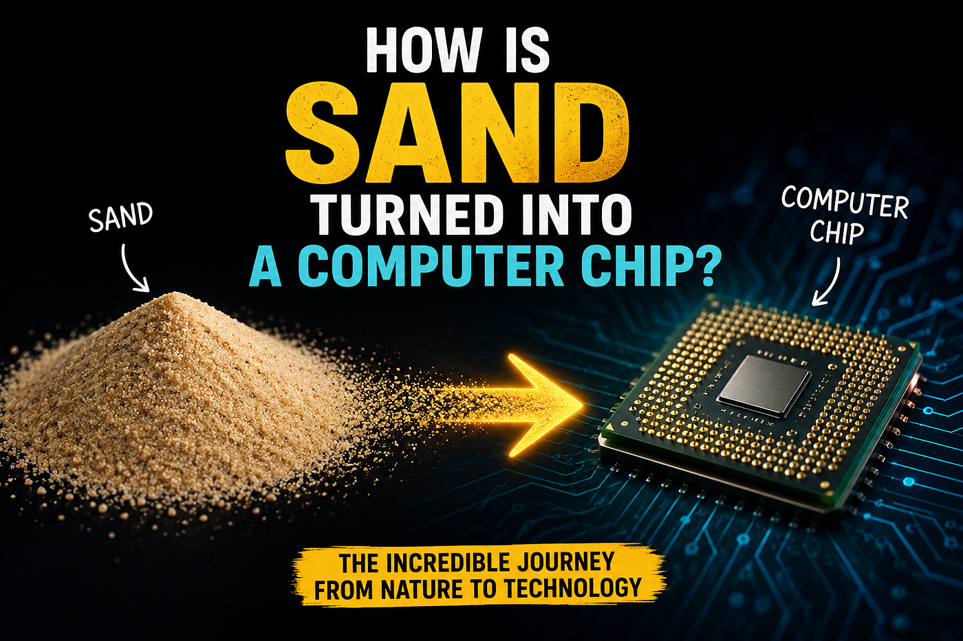
Take a look around you. Your smartphone. Your laptop. Your smartwatch. Your television. Even the servers powering today’s artificial intelligence. At the heart of each of these technologies is a semiconductor chip. But here’s a fascinating fact:
Every modern silicon chip begins its journey from silica (silicon dioxide), typically obtained from quartz-rich sand.
It sounds almost unbelievable that one of the world’s most advanced technologies starts with one of Earth’s most common raw materials.
So, how does silica become the powerful chip inside your devices?
Let’s explore the incredible journey.
It All Starts With Silica
Not all sand is suitable for making semiconductor chips.
The semiconductor industry uses silica (silicon dioxide, SiO₂), which is commonly obtained from quartz-rich sand.
Silicon is the second most abundant element in Earth’s crust after oxygen, making it an ideal material for semiconductor manufacturing.
However, the silicon found naturally in silica is chemically bonded to oxygen and is far from pure enough for electronic devices.
Before it can become the foundation of modern electronics, it must undergo several highly controlled manufacturing processes.
Step 1: Extracting Silicon
The first step is to separate silicon from silicon dioxide.
Quartz is heated with carbon in an electric arc furnace at extremely high temperatures.
This chemical reduction process removes oxygen from silicon dioxide, producing metallurgical-grade silicon, which is typically about 98–99% pure.
Although much purer than the original material, it still contains too many impurities for semiconductor manufacturing.
Step 2: Purifying the Silicon
Semiconductor manufacturing requires incredibly pure silicon.
Even tiny amounts of impurities can affect the electrical properties of semiconductor devices.
The metallurgical-grade silicon is therefore purified through additional chemical processes to produce electronic-grade silicon, typically with a purity greater than 99.9999999%.
This makes it one of the purest industrial materials produced anywhere in the world.
Step 3: Growing a Single Crystal
The purified silicon is melted inside a specialized furnace.
A small seed crystal is dipped into the molten silicon and slowly pulled upward while rotating.
This process, known as the Czochralski process, produces a large cylindrical single-crystal silicon ingot.
Using a single crystal is important because grain boundaries found in multi-crystal materials can interfere with the electrical performance of semiconductor devices.
Step 4: Slicing the Ingot into Wafers
The silicon ingot is sliced into thin circular discs called silicon wafers.
Each wafer is then carefully:
- Ground
- Lapped (when required)
- Polished
- Cleaned
until it has an ultra-flat, mirror-like surface.
These wafers provide the foundation on which integrated circuits are built.
Step 5: Building Billions of Tiny Devices
Now the real transformation begins.
Using advanced semiconductor fabrication techniques, engineers gradually build microscopic electronic devices and their interconnections onto the wafer.
Some of the major manufacturing processes include:
- Photolithography
- Thin-film deposition
- Etching
- Ion implantation
- Chemical Mechanical Planarization (CMP)
- Cleaning
- Inspection
These processes are repeated many times to build multiple layers of transistors and metal interconnects.
Depending on the product, modern processors and AI accelerators may contain tens of billions of transistors, while simpler chips may contain far fewer.
Step 6: Testing and Dicing
Once wafer fabrication is complete, every chip on the wafer undergoes electrical testing.
Chips that meet the required specifications move to the next stage.
The wafer is then cut into individual pieces in a process known as dicing.
Each individual piece of silicon is called a die.
Step 7: Packaging the Chip
A silicon die is delicate and cannot be used directly inside electronic products.
It is mounted inside a protective package that provides:
- Mechanical protection
- Electrical connections
- Heat dissipation
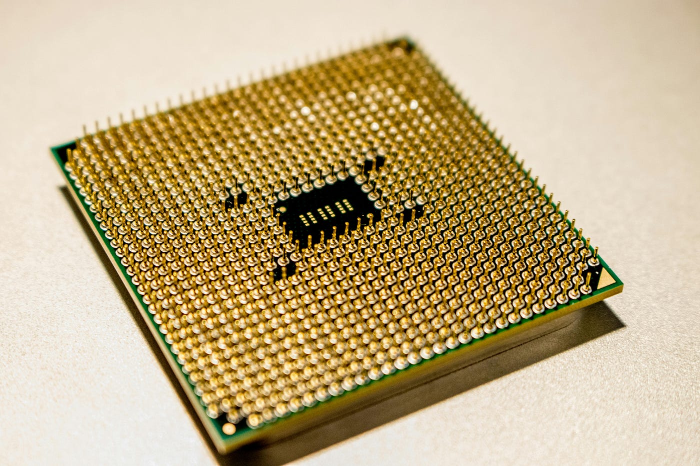
The packaged chip is then tested again before being integrated into products such as smartphones, laptops, automobiles, networking equipment, medical devices, and AI servers.
How Long Does It Take to Make a Chip?
Manufacturing a semiconductor chip is not a quick process.
Depending on the complexity of the device and the manufacturing flow, it can take several weeks to several months for a silicon wafer to complete fabrication, testing, packaging, and final quality checks.
This lengthy process reflects the extraordinary precision required at every stage.
Why Is Chip Manufacturing So Difficult?
Modern semiconductor manufacturing operates at dimensions measured in nanometers.
At this scale, even microscopic contamination can affect device performance.
To minimize defects, fabrication takes place inside highly controlled cleanrooms where:
- Airborne particles are carefully filtered.
- Temperature is tightly controlled.
- Humidity is regulated.
- Air pressure is maintained.
Every manufacturing step must be executed with exceptional precision to produce reliable chips.
Why Is Silicon Used?
Silicon has become the foundation of modern electronics for several reasons:
- It is abundant in Earth’s crust.
- It has excellent semiconductor properties.
- It forms a high-quality insulating oxide (silicon dioxide), which is essential for manufacturing many semiconductor devices.
- Decades of research and manufacturing expertise have created a mature global ecosystem around silicon technology.
Although researchers continue exploring alternative semiconductor materials for specialized applications, silicon remains the dominant material used in integrated circuits today.
From Quartz to Artificial Intelligence
The journey from quartz-rich sand to a semiconductor chip is one of the greatest achievements in modern engineering.
These tiny chips power:
- Smartphones
- Computers
- Medical equipment
- Satellites
- Communication networks
- Automobiles
- Cloud data centers
- Artificial intelligence systems
Without semiconductor chips, modern digital technology simply would not exist.
It’s remarkable to think that one of humanity’s most advanced technologies begins with silica obtained from quartz-rich sand.
Through purification, crystal growth, precision manufacturing, and advanced engineering, this ordinary raw material is transformed into semiconductor chips that power billions of electronic devices around the world.
The next time you unlock your phone, start your laptop, or ask an AI assistant a question, remember this:
Before it became the brain of your device, it began as silica extracted from quartz-rich sand — and through one of the most sophisticated manufacturing processes ever developed, it became the tiny chip powering the digital world.
메타데이터
- post_id
- db7dd5ccd8e2
- slug
- how-is-sand-turned-into-a-computer-chip-db7dd5ccd8e2
- url
- https://medium.com/silicon-circuits/how-is-sand-turned-into-a-computer-chip-db7dd5ccd8e2
- canonical_url
- https://medium.com/silicon-circuits/how-is-sand-turned-into-a-computer-chip-db7dd5ccd8e2
- author_url
- https://medium.com/@iamRadhaKulkarni
- status
- ok
- fetched_at
- 2026-06-28 14:26:31