What Is SLP PCB?
Substrate-Like PCB (SLP) technology is a revolutionary leap in the field of printed circuit boards that lies between standard PCBs and the…
What Is SLP PCB?
SLP PCB
Substrate-Like PCB (SLP) technology is a revolutionary leap in the field of printed circuit boards that lies between standard PCBs and the substrates used for semiconductors. This revolutionary technique has been widely recognized as a key enabler for next generation electronics production with high demand on space cost saving and three dimensional (3D) stacked modules. The engineer needs to know about **SLP PCB** manufacture if they want to design and build next generation electronic devices.
What is SLP technology?
**Substrate-Like PCBs** are designed for ultra-fine line and spacing 2 to 30 micrometers. In contrast to traditional PCBs, advanced materials and production techniques from the semiconductor industry are used in SLP boards manufacturing. The most noticeable benefit is the fact that SLP products can accommodate many more components without compromising electrical performance and reliability.
Basic Production Process
The SLP PCB production process begins with the preparation of specialized substrate materials, such as modified bismaleimide triazine resin systems. These materials exhibit excellent thermal stability and dimensional precision, which are required for processing ultra-fine features.
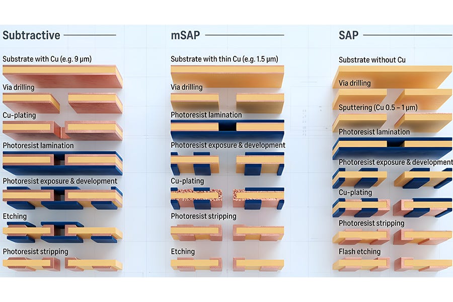
Patterning is a key stage of SLP PCB production. High-resolution photolithography techniques, similar to those used in semiconductor production, are utilized to develop accurate circuit designs. Direct laser writing systems with accuracy in the sub-micron range guarantee that the complex patterns are correctly mapped on the surface of the substrate.
SLP etching Ultra-fine traces must be maintained intact in the etching process of the SLP PCB production. Specialized etching chemistry and controlled environments inhibit undercutting and yield clean, sharply defined conductor designs. Continuous supervision and compensation are required at this stage in order to keep results uniform all over the plate.
Layer build up is also another important principle for SLP PCB production. Sequential lamination procedures are used, each layer is processed and laminated individually. This method provides for higher thickness control and better registration than traditional multilayer construction techniques.
Layer formation at the base of laser drilling creates the interconnections between layers. The process of SLP PCB manufacture use high-precision laser systems which can form vias as small as 25 micrometers in diameter. They are then metallized by special plating processes to make reliable electrical connections.
Surface finishing: SLP PCB manufacture contains the processes of ultra-thin protection coating and solderable finish. Traditional techniques such as electroless nickel immersion gold plating offer great surface planarity and solderability for the compliance to the fine pitch of high density designs.
Quality Control and Testing
Strict inspection procedures are part of the SLP PCB production. High spatial resolution automated optical inspection (AOI) system can find micro defects. Electrical testing confirms that the path is connected and measures the impedance to predict the best application in the end.
Frequently Asked Questions
What is the difference between SLP PCB manufacturing and regular PCB manufacturing?
SLP PCB production incorporates semiconductor-grade processes, ultra-fine lithography and special materials to provide significantly smaller feature sizes and higher interconnect density than traditional PCB production.
What are the best application for SLP technology?
Smartphones, Tablets, Wearable, Automotive, and High Performance Compute (HPC) use SLP PCBs extensively for their small size and high electrical performance.
What are the key challenges in SLP PCB production?
Key issues are achieving yield in ultra-fine features, dealing with differences in thermal expansion, and ensuring uniformity over large production quantities.
Are the costs between SLP and regular PCBs similar?
SLP PCB manufacturing is generally costly because of the special equipment and materials as well as processes needed, but the advantages in device miniaturization and performance usually make it worthwhile.
What are the future prospects of SLP technology?
Further miniaturization in the form of finer line widths, better materials and higher productivity will lead the next generation SLP PCB manufacturing.
메타데이터
- post_id
- e322f0213050
- slug
- what-is-slp-pcb-e322f0213050
- url
- https://medium.com/@wyg28291/what-is-slp-pcb-e322f0213050
- canonical_url
- https://medium.com/@wyg28291/what-is-slp-pcb-e322f0213050
- author_url
- https://medium.com/@wyg28291
- status
- ok
- fetched_at
- 2026-06-17 08:20:12