Co-Packaged Optics Is Killing Traditional PCBs — A Technology Inflection Point Every Hardware…
When NVIDIA announced mass production of its Spectrum-X Ethernet silicon photonics platform at Computex 2026, most people in the audience…
Co-Packaged Optics Is Killing Traditional PCBs — A Technology Inflection Point Every Hardware Engineer Must Know in 2026
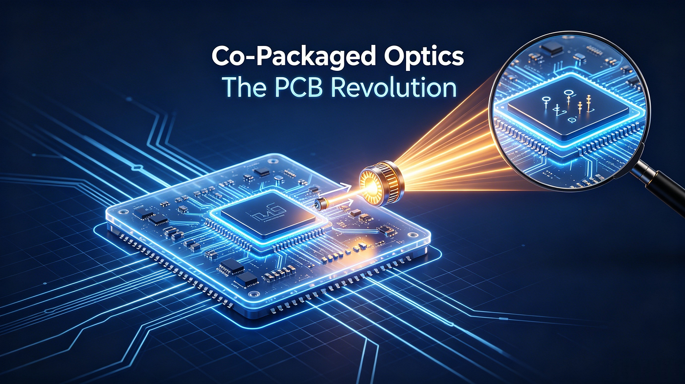
When NVIDIA announced mass production of its Spectrum-X Ethernet silicon photonics platform at Computex 2026, most people in the audience focused on one number: port power dropped from 14‑16W to just 5.5W.
But the real shockwave for the PCB industry was hidden in a less flashy sentence: the optical engine and switching chip are packaged on the same substrate, and the electrical signal distance from chip to optical interface shrinks from centimeters to micrometers.
What does that mean? It means the fundamental logic that the PCB industry has built over the past few decades — transmitting high‑speed electrical signals over copper traces — is being rewritten.
This is not another AI article — you’ve read enough of those. This is a technical deep dive into how PCBs are evolving from “electrical bridges” to “optical infrastructure”. A silent, irreversible revolution that every hardware engineer must face.
1. CPO Is No Longer a Concept — It’s Already in Mass Production
Before diving into the technology, let’s state a fact: CPO (co‑packaged optics) is no longer a lab experiment.
In Q1 2026, Broadcom launched the first 51.2Tbps CPO switch, Bailly, integrating 64 optical engines that switch light directly. Its rival Marvell released a similar 51.2T CPO platform at the same time. Two major players entering mass production simultaneously marks that CPO has officially left the validation phase.
NVIDIA’s Spectrum‑X — an Ethernet switch platform based on CPO — also reached mass production in 2026. According to industry reports, optical interconnect technologies like CPO and OCS (optical circuit switching) will see large‑scale deployment in 2026, becoming a core direction for AI data center infrastructure upgrades.
These events send a clear signal: light is replacing electricity as the primary interconnect within data centers.
2. How CPO Works — A Quick Engineering Primer
If you’re not familiar with CPO, here’s the fastest explanation of the problem it solves:
Traditional data center: Switching chip → electrical signal over PCB traces → SerDes → pluggable optical module → optical signal. Long path, high loss, high power.
CPO: The switching chip and optical engine are packaged on the same substrate, with the optical engine just micrometers away from the chip. The electrical signal is converted to light almost instantly, without traversing PCB traces.
Result: Port power drops from 14‑16W to about 5.5W, with significant reductions in signal loss and latency. The electrical signal path from chip to optical interface is shortened by more than 100×, virtually eliminating parasitic effects.
For data center operators obsessed with energy efficiency, that number is enough to replace every pluggable optical module.
3. PCB’s “Dethronement” and “Rebirth” — Why CPO Is a Watershed
The impact of CPO on the PCB industry can be understood from two perspectives.
3.1 PCB’s “Dethronement”: Signals No Longer Travel on the Board
In traditional data centers, the switching chip and optical modules were connected via PCB traces. Complex high‑speed signal routing was a core value driver for PCBs.
In a CPO architecture, that routing is absorbed inside the package. A large number of high‑speed signals disappear from the PCB surface.
What does that mean? The “status” of PCBs in core data center switching equipment is declining. PCBs no longer carry the most critical signals, retreating to roles like power distribution, low‑speed management, and mechanical support. For PCB manufacturers that depend on high‑speed signal complexity, this is a fundamental challenge.
3.2 PCB’s “Rebirth”: EOCB Is Coming
But the story doesn’t end there. PCBs won’t disappear — they will evolve.
A new concept is quietly emerging: EOCB (Embedded Optical Circuit Board) .
EOCB is not simply stuffing optical fibers into a circuit board. It involves building optical waveguides inside or on the surface of the PCB dielectric layer, embedding optical paths into the PCB structure so that light and electricity coexist on the same board. According to industry research, one of the evolutionary directions of PCB technology is “optical‑copper integration” — EOCB actively integrates co‑packaged optics, with optical paths realized by lasers, fibers, waveguides, and polarization components.
In other words, PCBs are moving from “conducting only electricity” to “guiding both light and electricity” .
This demands entirely new manufacturing capabilities:
- Waveguide fabrication precision — Light has much smaller wavelengths than electrical signals. PCBs must learn to “guide” light.
- Material property matching — The refractive index and thermal performance of optical waveguide materials must match those of copper routing layers.
- Higher process accuracy — Precisely building micron‑scale optical structures inside a PCB is a brand‑new challenge for traditional PCB fabs.
Industry outlooks point to EOCB as an important direction for PCB technology evolution, with some leading PCB manufacturers already beginning to adopt related processes.
4. Embedded Passives — Another Quiet Revolution Inside the PCB
While we’re talking about the convergence of light and electricity, another equally profound revolution is happening inside the PCB: embedded passive components.
4.1 What is it?
Traditionally, passive components like resistors, capacitors, and inductors are placed on the PCB surface (SMT). These components occupy 30‑50% of the board area and account for a similar percentage of solder joints — each joint representing a potential reliability risk. Embedded passive technology builds these components directly inside the PCB dielectric layer, consuming no surface space.
According to technical literature, one of the original goals of embedded passive technology was to embed at least 30‑50% of the passives used in wireless and portable products, reducing component count, shrinking board size, and lowering product cost.
4.2 Key advantages
- Board space savings — Embed small resistors and capacitors, leaving surface area for critical ICs and connectors.
- Improved high‑frequency signal integrity — Embedded components are integrated directly into inner layers, offering significantly lower parasitic inductance than SMT. High‑frequency signal paths are dramatically shortened, with especially noticeable improvements at RF and millimeter‑wave frequencies.
- Enhanced system reliability — Eliminating a large number of surface solder joints reduces failure points under vibration and thermal cycling.
4.3 Where are the challenges?
Of course, the technology is not without hurdles. The electrical performance of embedded passives ultimately depends on geometric alignment accuracy with the signal traces and reference planes above and below. High‑precision registration, material compatibility, thermal expansion matching, and cost control are the main obstacles. But like all technologies migrating from high‑end to mainstream, these engineering challenges are gradually being overcome.
5. Implications for Hardware Engineers and Small‑Batch Manufacturers
5.1 For hardware engineers: your design flow needs updating
When PCBs start carrying both light and electricity, and embedding passive components, traditional design flows no longer suffice.
- For CPO/EOCB designs — you’ll need to discuss waveguide materials, optical interface connections, and how to interface with optical chip packages with your PCB manufacturer. Traditional high‑speed SerDes knowledge is still valuable, but no longer enough.
- For embedded passive designs — you need to learn how to select, place, and match embedded resistors/capacitors, and confirm the manufacturer’s embedded layer capabilities in advance.
- The importance of early collaboration — As one industry expert noted, advanced technology “is not the kind of thing you can just throw over the wall”. “Without upfront collaboration, you’ll face delays, redesigns, and rework.”
5.2 For small‑batch manufacturers: barriers are rising, but opportunities are diverging
The increased precision required by CPO and embedded passives is accelerating the fragmentation of the PCB industry. Barriers are rising — some small‑batch manufacturers may be squeezed out of the high‑end market. But this also means that manufacturers who master these new processes first will establish a near‑insurmountable technical moat, earning far higher pricing power and customer loyalty than traditional players.
At the same time, new technologies like CPO and EOCB require extensive prototyping, test boards, and small‑batch orders for validation and early adoption. That is the natural home of flexible, small‑batch manufacturers.
6. How AnyPCBA Is Responding to These Technology Shifts
**AnyPCBA**, founded in 2011, specializes in small‑to‑medium batch (5–5,000 pieces) PCB fabrication and PCBA assembly. In the face of CPO and embedded passives, we are preparing from several directions:
- Understanding process requirements — We continuously track PCB‑related technologies for CPO: EOCB optical waveguide integration, ultra‑precision laser drilling, ultra‑flat surface finishes. When you need test boards or carriers for CPO modules, we can offer professional advice based on real manufacturing experience.
- Precision capability reserves — We are actively responding to UHDI (ultra‑high‑density interconnect) processes. UHDI generally refers to micro‑vias <75µm, line/space <50µm, and dielectric thickness in the same 50µm range — an order of magnitude finer than traditional HDI. We are gradually improving our manufacturing precision in line with industry trends.
- Monitoring embedded technology — We keep a close watch on the maturity of embedded passives (embedded resistors/capacitors). When customer designs start incorporating embedded components, we will be able to accurately assess manufacturing feasibility and potential yield risks.
We don’t claim to be a “mass‑production leader” of any “cutting‑edge technology” — that’s not our position. Our promise is: when your designs begin adopting new processes, we can quickly understand your requirements, accurately evaluate process capabilities, and deliver reliably at small‑to‑medium batch volumes. In an era of increasingly complex technology and materials, a stable, flexible partner who is willing to walk with you from test board to production is more valuable than ever.
*AnyPCBA — Small‑to‑medium batch PCB & PCBA. If you’re exploring CPO, EOCB, or next‑generation high‑density designs, let’s talk about your process needs.*
👉 AnyPCBA website: https://www.anypcba.com/
메타데이터
- post_id
- e8f7bbd8d71c
- slug
- co-packaged-optics-is-killing-traditional-pcbs-a-technology-inflection-point-every-hardware-e8f7bbd8d71c
- url
- https://medium.com/@AnyPCBA_Official/co-packaged-optics-is-killing-traditional-pcbs-a-technology-inflection-point-every-hardware-e8f7bbd8d71c
- canonical_url
- https://medium.com/@AnyPCBA_Official/co-packaged-optics-is-killing-traditional-pcbs-a-technology-inflection-point-every-hardware-e8f7bbd8d71c
- author_url
- https://medium.com/@AnyPCBA_Official
- status
- ok
- fetched_at
- 2026-06-12 22:02:08