A Methodology for Optimizing Decoupling (DECAP) Cell Placement to Reduce Leakage Power
Author : Asmaa Sameh — Hardening Engineer , Si-Vision
A Methodology for Optimizing Decoupling (DECAP) Cell Placement to Reduce Leakage Power
Author : Asmaa Sameh — Hardening Engineer , Si-Vision
Introduction: The Challenge of Power Integrity in Modern IC Design
Managing power integrity is a strategic imperative in the design of complex digital integrated circuits. As device complexity increases and operating voltages decrease, mitigating dynamic IR drop — the transient voltage drop on the power delivery network — has become a critical challenge. Failure to control this drop can increase gate delays, causing timing violations that compromise performance and ultimately lead to functional failure, making it a primary focus for design engineers seeking to ensure device reliability.
As shown in the transient analysis below (Figure 1), how the Core Voltage (Vcore) sags while System Ground (SGND) simultaneously rises during a switching event.
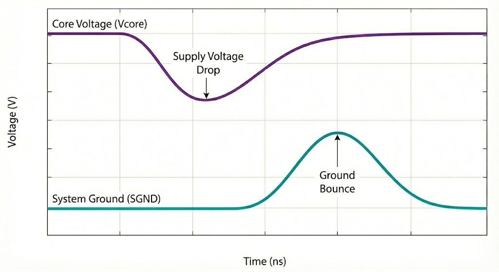
Figure 1. Voltage Drop on the VDD rail and Ground Bounce on the GND rail
The industry-standard practice to address dynamic IR drop involves the strategic use of decoupling (DECAP) cells. These cells are essentially small capacitors placed within the digital implementation area, acting as localized charge reservoirs. When nearby functional cells switch, drawing a sudden burst of current, the DECAP cells supply this immediate demand, stabilizing the local power rail and minimizing the resulting voltage drop. Figure 2 shows a schematic representation of a CMOS inverter chain with integrated decoupling. The diagram illustrates a decoupling capacitor placed in parallel with the switching logic to provide local transient currents , thereby mitigating simultaneous switching noise on the Vdd (Vcore) and Vss (SGND) supply rails.

Figure 2. Mitigation of voltage droop and ground bounce via decoupling
However, a common inefficiency has emerged from a design practice driven more by layout convenience than by electrical necessity. In an effort to fill layout gaps and achieve high design utilization (often targeting 100%), designers frequently resort to “massively placing” DECAP cells throughout the design. The negative consequence of this approach is a significant increase in leakage power. Many of these filler DECAP cells are placed in locations where they do not contribute meaningfully to mitigating IR drop, yet they continuously consume power. This needless power consumption demands a more precise, analytical method to validate the effectiveness of each DECAP cell, ensuring that only necessary components remain in the final design.
2. The Function and Strategic Placement of DECAP Cells
At their core, DECAP cells function as localized voltage sources strategically positioned within the layout to support the power grid. They are typically placed in the digital implementation area, interspersed between functional standard (STD) cells. This proximity allows them to respond almost instantaneously to the high-frequency current demands of switching logic, preventing the local supply voltage from collapsing.
The placement of DECAP cells is most critical in the vicinity of cells with a high toggle rate. Components like clock cells and isolation (ISO) cells are particularly demanding on the power delivery network due to their frequent and predictable switching activity. Effective placement ensures that these high-activity cells have immediate access to a stable charge supply, minimizing fluctuations in the effective voltage and keeping it safely above the required operational threshold, thereby ensuring the predictable switching speeds required for stable timing.
While the theoretical importance of DECAP cells is well-established, the practical challenge lies in avoiding their overuse. This gap between targeted, strategic placement and the widespread use of DECAPs as simple filler cells necessitates an empirical approach to identify and eliminate waste.
3. A Proposed Methodology for Evaluating DECAP Cell Effectiveness
To address the power inefficiency stemming from excessive DECAP cell usage, this paper proposes an experimental framework for empirical validation. The objective of this methodology is to provide a data-driven way to distinguish between DECAP cells that are actively contributing to power integrity and those that are redundant, serving only as a source of leakage power. As shown in Figure 3. which is a heatmap representation of an IP placement grid highlighting an IR drop violation region. The central, multi-site red block is identified as a “Violated IR cell,” indicating excessive voltage drop. It is immediately surrounded by a cluster of decoupling capacitor (DCAP) cells (shown in different tones which describes the voltage drop on each based on the support to the violated surrounding cell) deployed to mitigate the power supply noise in that specific area.

Figure 3. Physical design view of IR drop mitigation.
The core premise of the experiment involves analyzing the real-time electrical behavior of individual DECAP cells under operational conditions. Using a specialized tool such as ANSYS Redhawk-SeaScape, an engineer can probe the voltage of a specific DECAP cell and monitor its waveform over time. The characteristics of this waveform serve as a direct indicator of the cell’s utility and effectiveness.
The criteria for interpreting the waveform data are clear and binary:
- Indicator of an Effective DECAP A waveform that changes rapidly over time and exhibits significant ripples is the signature of a DECAP cell that is actively contributing to power rail stability. This behavior indicates that the cell is actively charging and discharging to supply current to nearby switching logic, directly compensating for drops on the power rail and fulfilling its intended purpose.
- Indicator of an Ineffective (Useless) DECAP Conversely, a waveform that remains almost stable with a constant voltage implies the DECAP cell is not participating in any significant electrical activity. This stability suggests that there are no nearby high-current events for it to service. Such a cell is functionally useless and can be safely removed from the design to recover the leakage power it needlessly consumes.
Figure4. Proposed algorithmic workflow for generating placement-aware IR drop heatmaps. The process initiates with the ingestion of decoupling capacitor (DCAP) instance data, followed by parallel execution paths to extract spatial coordinates and calculate site-specific voltage differentials. The final stage correlates these datasets to visualize localized power integrity signatures within the ASIC placement grid. as showen in table 1 how replace the unsupportive DCAP with fill cell improve the leakage power by around 30%

Figure 4. Workflow for automated IR drop heatmap generation.

Table 1. Summary of leakage power and percentage results for experimental trials.
4. Conclusion: A Path to Optimized Power Management
The indiscriminate placement of decoupling cells, often done to achieve layout completion targets, is a significant and entirely avoidable source of leakage power in modern integrated circuits. This practice, while convenient, directly undermines power efficiency goals by populating designs with components that offer no functional benefit.
The primary advantage of applying the proposed methodology is clear and impactful. By leveraging waveform analysis to systematically identify and remove redundant or “useless” DECAP cells, design teams can achieve a significant reduction in overall leakage power. Crucially, this optimization can be performed without compromising the power integrity of the design, as only the non-contributing cells are targeted for removal.
Ultimately, this data-driven methodology represents a more intelligent and efficient strategy for power management. By validating the purpose of every component, designers can move beyond brute-force techniques and embrace a precision-oriented approach that is essential for developing the next generation of high-performance, power-efficient semiconductors.
메타데이터
- post_id
- e9850d240ca4
- slug
- a-methodology-for-optimizing-decoupling-decap-cell-placement-to-reduce-leakage-power-e9850d240ca4
- url
- https://medium.com/si-vision-tech-blog/a-methodology-for-optimizing-decoupling-decap-cell-placement-to-reduce-leakage-power-e9850d240ca4
- canonical_url
- https://medium.com/si-vision-tech-blog/a-methodology-for-optimizing-decoupling-decap-cell-placement-to-reduce-leakage-power-e9850d240ca4
- author_url
- https://medium.com/@asmaa.sameh
- status
- ok
- fetched_at
- 2026-06-14 11:28:49