How to Depanel Mobile Phone Power Adapter PCBs Without Damaging Components
Mobile phone power adapter manufacturing has always been a space where precision matters.
How to Depanel Mobile Phone Power Adapter PCBs Without Damaging Components
Mobile phone power adapter manufacturing has always been a space where precision matters.
But in recent years, the challenge has become even more demanding.
As electronic devices continue to shrink while performance requirements increase, PCB designs inside power adapters are becoming:
- More compact
- More densely populated
- More sensitive to mechanical stress
This evolution has a direct impact on one critical manufacturing step:
Why Depaneling Matters More Than Ever
At first glance, depaneling may look like a simple step in production — just separating individual boards from a panel.
However, in reality, it plays a crucial role in determining product quality and long-term reliability.
In mobile phone power adapter PCB production, even small mechanical stress during cutting can lead to serious issues, such as:
❌ Micro-cracks in the PCB structure ❌ Damage to sensitive components ❌ Solder joint weakening ❌ Hidden reliability failures ❌ Reduced production yield
The problem is that many of these defects are not immediately visible.
They often appear later in testing or even after the product has been shipped.
The Challenge of High-Density Power Adapter PCBs
Modern power adapter PCBs are designed with efficiency and space optimization in mind.
This often means:
- Components placed closer to board edges
- Narrower spacing between sensitive parts
- Thinner PCB structures
- Higher functional integration on a smaller footprint
While this improves product performance and compactness, it also increases vulnerability during mechanical processing.
Traditional depaneling methods can introduce stress that these compact designs are not always able to tolerate.
Moving Toward Low-Stress PCB Routing
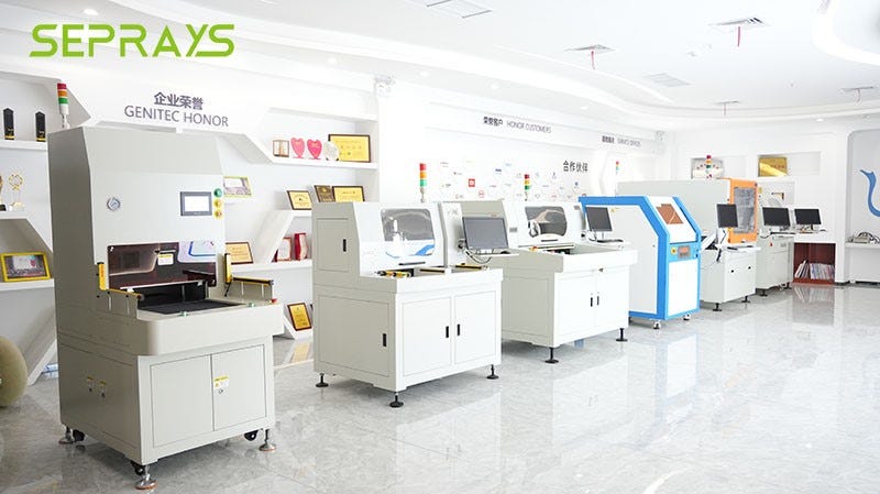
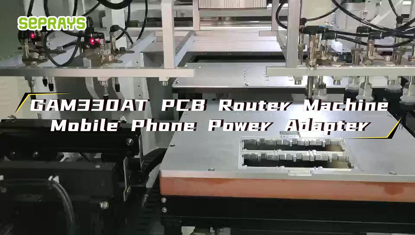
To address these challenges, many manufacturers are adopting low-stress PCB routing solutions, such as the GAM330AT PCB Router Machine.
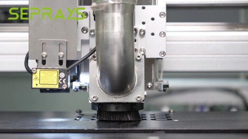
Instead of relying on force-based separation, routing systems use controlled cutting paths designed to minimize mechanical impact.
Key Advantages of Low-Stress Routing
✔ Reduced mechanical stress during cutting ✔ Higher precision in separation paths ✔ Better protection for edge-close components ✔ Improved consistency in mass production ✔ Lower risk of hidden defects
These benefits are especially important for power adapter PCBs, where reliability and safety are critical.
Why GAM330AT Is Used in Power Adapter Applications
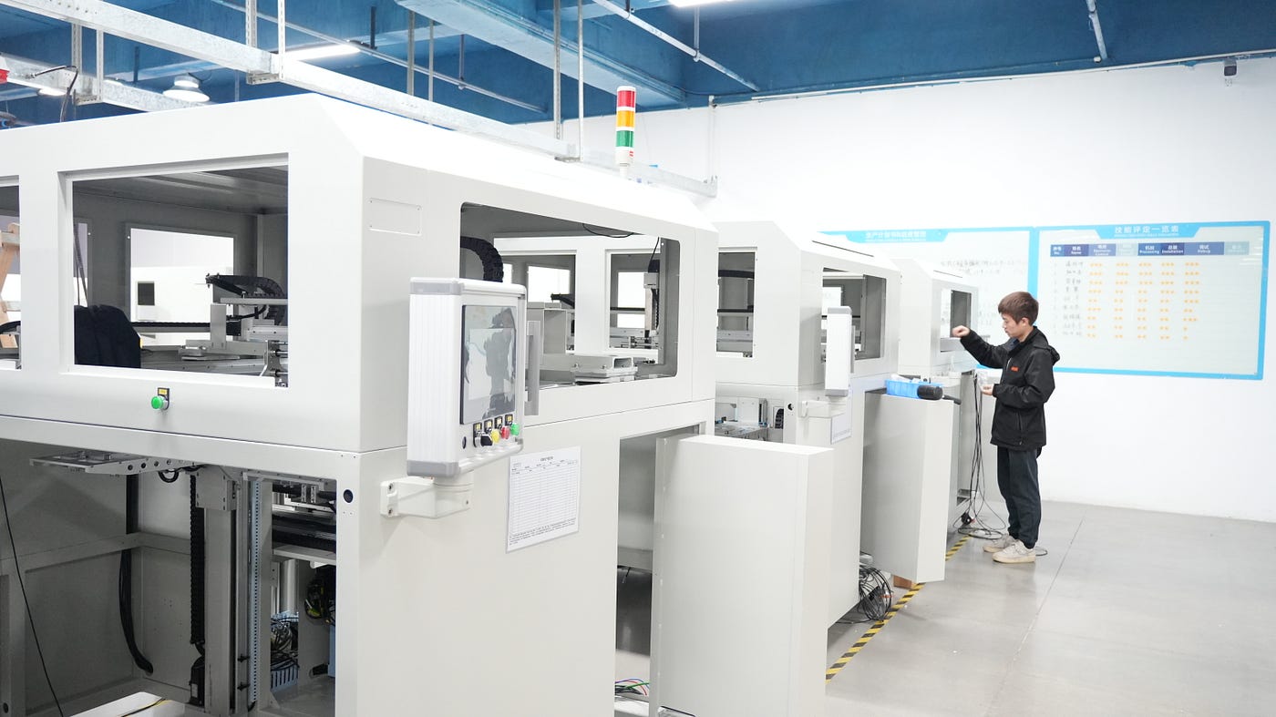
The **GAM330AT PCB Router Machine** is designed specifically for precision depaneling environments where stability and accuracy are required.
In mobile phone power adapter production, it helps manufacturers:
- Maintain cutting accuracy on compact layouts
- Reduce stress impact on sensitive components
- Improve yield rates in high-volume production
- Ensure consistent separation quality across batches
As production scales increase, process stability becomes just as important as cutting speed.
From Cutting to Quality Protection
One of the most important shifts in PCB manufacturing today is the way depaneling is being viewed.
It is no longer just a mechanical separation step.
Instead, it is increasingly seen as part of the quality protection process.
Manufacturers are now focusing on:
- Preventing defects rather than detecting them later
- Reducing stress before it becomes a reliability issue
- Ensuring consistency across every unit produced
This shift is especially important in high-volume consumer electronics like mobile phone power adapters.
Final Thoughts
Depaneling may seem like a small step in the production process, but its impact is significant.
For mobile phone power adapter PCBs, the challenge is not just separating boards efficiently — it is doing so without compromising product integrity.
Low-stress routing solutions such as GAM330AT provide a practical way to balance:
✔ Precision ✔ Stability ✔ Yield ✔ Long-term reliability
As PCB designs continue to evolve, the importance of controlled, low-stress depaneling will only continue to grow.
Read more here:
메타데이터
- post_id
- ed2e07965622
- slug
- how-to-depanel-mobile-phone-power-adapter-pcbs-without-damaging-components-ed2e07965622
- url
- https://medium.com/@sales_40837/how-to-depanel-mobile-phone-power-adapter-pcbs-without-damaging-components-ed2e07965622
- canonical_url
- https://medium.com/@sales_40837/how-to-depanel-mobile-phone-power-adapter-pcbs-without-damaging-components-ed2e07965622
- author_url
- https://medium.com/@sales_40837
- status
- ok
- fetched_at
- 2026-06-20 20:29:01