IC Substrate Manufacturing Technology Guide (2025)
The semiconductor development is developing quickly; the IC substrate manufacturing acts as the advanced packaging of the newest devices…
IC Substrate Manufacturing Technology Guide (2025)
IC substrate
The semiconductor development is developing quickly; the IC substrate manufacturing acts as the advanced packaging of the newest devices. In the quest to drive further into 2025, it is likely that appreciating the complexity of processes behind IC substrate manufacturing is going to become increasingly important for engineers, makers and tech fans alike. A comprehensive guide to the innovative new methods for IC substrates: IC Substrate Fabrication Technology addresses cutting-edge solution methods for IC substrates — along with real-world manufacturing challenges.
Understanding IC Substrate Manufacturing Fundamentals
The manufacture of IC substrates is a complex combination of materials science, precision engineering and state-of-the-art production processes. Such substrates are important intermediate layers between the semiconductor die and the printed circuit board, providing electrical connections along with mechanical support and thermal control. Because of increasing needs on performance, size reduction and cost reduction, the complexity of the current IC substrate fabrication increased amazingly. Industry reports by Prismark Partners indicate that the total IC substrate market was $15.2 billion in 2024 and forecast the trend will increase beyond 2025. This growth is representative of the growing demands made on IC substrate fabrication technology in order to satisfy demands for advancing technology.
Core Manufacturing Process Flow
Material Preparation and Selection
The foundation of successful IC substrate manufacturing begins with meticulous material selection. Engineers typically choose from several substrate materials, each offering distinct advantages. Bismaleimide-triazine (BT) resin remains the preferred choice for high-performance applications, offering superior thermal stability and electrical properties. Advanced polyimide materials are increasingly utilized in flexible substrate applications, while ceramic substrates excel in high-power and high-frequency scenarios.
Material preparation involves precise control of resin content, fiber weave patterns, and surface treatments. Quality control measures during this phase directly impact the final substrate’s reliability and performance characteristics.
Layer Stackup Design and Engineering
Modern IC substrate manufacturing requires sophisticated layer stackup designs to accommodate complex routing requirements. Engineers utilize advanced simulation software to optimize signal integrity, power distribution, and thermal management. The stackup design process considers factors such as impedance control, crosstalk minimization, and via placement optimization.
Industry data from IPC indicates that typical high-density substrates now feature 8–16 layers, with some advanced applications requiring up to 20 layers. This complexity necessitates precise manufacturing control throughout the IC substrate manufacturing process.
Lamination Technology and Process Control
The lamination stage represents a critical juncture in IC substrate manufacturing, where multiple prepreg and core layers are bonded under carefully controlled temperature and pressure conditions. Modern lamination presses feature advanced heating profiles and pressure distribution systems to ensure uniform bonding across the entire substrate panel.
Temperature profiles typically range from 170°C to 200°C, with pressure applications reaching 400–600 PSI. Process monitoring systems continuously track parameters to maintain consistency and prevent defects such as delamination or void formation.
Advanced Drilling Technologies
Precision drilling forms the foundation for interconnection in IC substrate manufacturing. Contemporary facilities employ multiple drilling technologies to achieve varying via requirements. Mechanical drilling handles larger diameter vias, while laser drilling systems create microvias with diameters as small as 25 micrometers.
Recent advancements in laser drilling technology have enabled aspect ratios exceeding 10:1, significantly enhancing design flexibility in IC substrate manufacturing. UV laser systems operating at 355nm wavelengths provide exceptional precision for creating blind and buried vias in multilayer constructions.
Metallization and Plating Processes
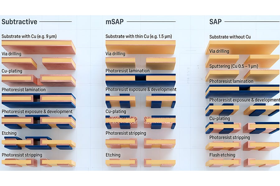
The metallization phase in IC substrate manufacturing involves depositing conductive materials to establish electrical pathways. Electroless copper deposition initiates the process, followed by electrolytic copper plating to achieve desired thickness specifications. Advanced plating systems maintain precise current density control and solution chemistry to ensure uniform copper distribution.
Modern IC substrate manufacturing facilities achieve copper thickness tolerances of ±10% across substrate panels, meeting stringent electrical performance requirements. Surface finish options include HASL, ENIG, and OSP, each selected based on specific application requirements.
Pattern Definition and Etching
Photolithography processes define circuit patterns with exceptional precision in IC substrate manufacturing. Advanced exposure systems utilize LED-based light sources for improved uniformity and reduced processing times. Resist materials are carefully selected to achieve optimal resolution and etch resistance.
Etching processes remove unwanted copper while preserving circuit patterns. Modern etching equipment features precise spray pressure control and solution recycling systems to maintain consistent results throughout production runs.
Quality Assurance and Testing Protocols
Quality control represents a fundamental aspect of IC substrate manufacturing, with multiple inspection stages ensuring product reliability. Automated optical inspection (AOI) systems examine surface features with microscopic precision, identifying defects such as shorts, opens, or dimensional variations.
Electrical testing validates connectivity and impedance characteristics using specialized test equipment. In-circuit testing verifies each electrical path, while impedance measurements ensure signal integrity compliance. Statistical process control methods track key parameters throughout IC substrate manufacturing operations.
Emerging Technologies and Innovations
Advanced Materials Integration
The integration of novel materials continues to drive innovation in IC substrate manufacturing. Low-loss dielectric materials enable higher frequency applications, while thermally conductive substrates address heat dissipation challenges in high-power devices. Embedded component technologies integrate passive components directly within substrate layers, reducing overall system size and improving performance.
Manufacturing Automation
Automation technologies are revolutionizing IC substrate manufacturing efficiency and consistency. Robotic handling systems minimize human contact, reducing contamination risks and improving yield rates. Machine learning algorithms optimize process parameters in real-time, adapting to material variations and environmental conditions.
Sustainability Initiatives
Environmental considerations increasingly influence IC substrate manufacturing practices. Water recycling systems reduce consumption by up to 80%, while advanced chemical recovery processes minimize waste generation. Energy-efficient equipment and renewable power sources contribute to reduced carbon footprints in modern manufacturing facilities.
Frequently Asked Questions
What factors determine the choice of substrate material in IC substrate manufacturing?
Material selection depends on application requirements including operating frequency, power dissipation, mechanical stress, and cost constraints. BT resin offers excellent electrical properties for high-performance applications, while FR-4 provides cost-effective solutions for standard requirements.
How do manufacturers ensure quality consistency in IC substrate manufacturing?
Quality consistency relies on statistical process control, automated inspection systems, and rigorous testing protocols. Real-time monitoring systems track critical parameters, while feedback loops enable immediate process adjustments to maintain specifications.
What are the typical lead times for IC substrate manufacturing?
Standard substrates typically require 2–3 weeks for production, while complex designs may extend to 4–6 weeks. Prototype quantities often receive expedited processing with lead times of 5–7 days.
How does IC substrate manufacturing address miniaturization trends?
Shrinking favors growth for HDI technologies, high aspect ratio drilling, and thinner materials. Equipment companies and the like invest in equipment for guiding, etc in a processing of a much finer pattern without lowering a reliability.
The future of **IC substrate production** holds a great deal of innovation ahead as industry needs change. New materials, robotics and green initiatives will drive a new era of manufacturing, and help the industry maintain its pace with the always-on global market.
메타데이터
- post_id
- f2ea8be6b5f9
- slug
- ic-substrate-manufacturing-technology-guide-2025-f2ea8be6b5f9
- url
- https://medium.com/@wyg28291/ic-substrate-manufacturing-technology-guide-2025-f2ea8be6b5f9
- canonical_url
- https://medium.com/@wyg28291/ic-substrate-manufacturing-technology-guide-2025-f2ea8be6b5f9
- author_url
- https://medium.com/@wyg28291
- status
- ok
- fetched_at
- 2026-07-28 00:39:46