Designing a deglitch filter in xschem
What is a glitch? In this article, we'll design a simple circuit which can help in filtering unwanted signal transitions.
Designing a deglitch filter
Introduction
In digital and mixed-signal systems, signals can often contain unwanted short-duration spikes, often referred to as glitches. They can cause false triggering in logic circuits and corrupt data. A deglitch filter is a practical solution to clean up these signals by filtering out glitches.
In this post, I’ll walk you through designing a deglitch filter from scratch using **IIC-OSIC-TOOLS**: xschem for schematic capture and ngspice for simulation. All files, schematics, and measurements are available as a GitHub repository. Feel free to replicate, modify, or build upon the design.
Implementation
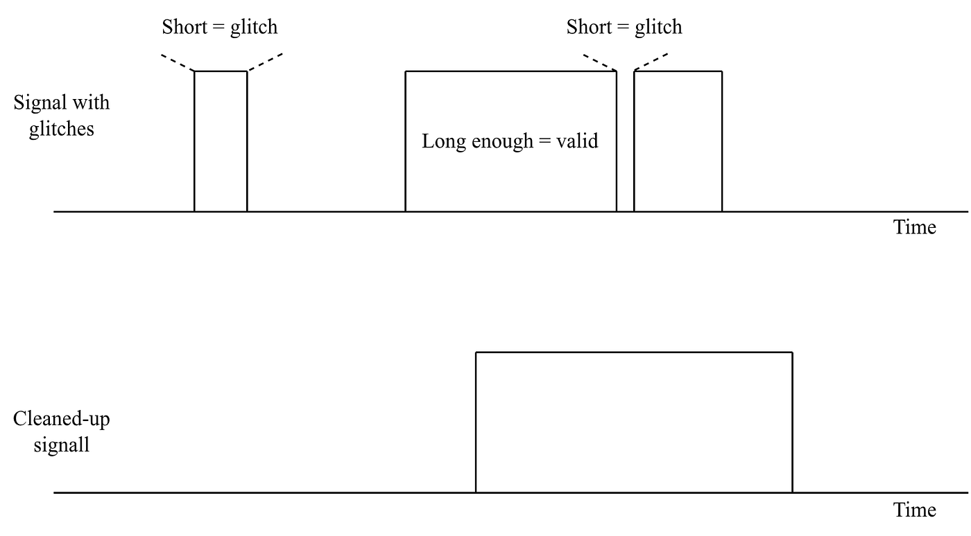
A glitch is a short-duration spike or a drop in our signal. So, we can derive a simple criterion to differentiate a glitch from a valid signal, which is time. A signal is a glitch if it holds a state shorter than a specific time period. Otherwise, it’s a valid signal. Applying this criterion to a signal, we can clean it up from glitches by simply waiting to see if a signal change is long enough and then changing the output. So, a deglitch filter is a delay.
Design and implementation
A simple deglitch filter can be implemented using an RC-based delay cell.

In this circuit, the input voltage (v_i) controls the charging or discharging of an RC circuit connected between v_drv and v_cap nodes. The voltage on the v_cap node is monitored by a Schmitt trigger-based comparator. You can find more on this design here. The signal polarity at the output of the circuit is matched to the polarity at the input using an additional inverter.
The total deglitch time (delay time) of this circuit is mostly dominated by the RC constant and the thresholds of the Schmitt trigger. The propagation delay of the additional digital cells in the circuit (inverters) adds some delay as well. In the above circuit, the deglitch time is set to approx. 100 ns.
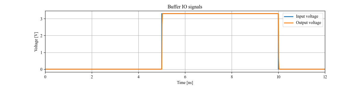
The circuit performance can be tested by applying a pulse at the input. The pulse length should be longer than the desired deglitch time. What can be measured is the propagation delay between the rising/falling edges between the output and the input. This time delta is the deglitch time of the filter.
Design considerations
Some considerations should be noted in this design:
- The previously shown design has two MOS capacitors from the v_cap nodes to the VDD and VSS nodes. In my experience, this design is easier to tune for symmetric delay times between rising and falling input signals. These delay times normally vary due to the differences in non-linear capacitive loading of different nodes to the supply or the ground, different driving strengths of PMOS/NMOS drivers, non-symmetric thresholds of the Schmitt trigger, etc.
- The resistance value in the RC filter scales by length, while the capacitor value scales by area. So, my preference is to make the resistance more dominant in the circuit due to a lower area penalty. Take note not to use too small a capacitance as it will be more impacted by parasitic capacitances from the metal interconnects. Aim for a low capacitance that is still more dominant with respect to the additional parasitic capacitances.
Design improvements
Using the presented design works well for quasi-static signals, where the state doesn't change often. However, this circuit has a potential pitfall in signals that change states more often.
The deglitch time of the circuit is dependent only on a part of the RC constant. It is limited by the threshold voltage of the Schmitt trigger. Once the Schmitt trigger detects a level change, it will propagate it to the output. The voltage on the v_cap node will still keep charging/discharging. If the input signal changes its state before the full charge/discharge is complete, the v_cap node is being charged/discharged from an intermediate value, not from its DC value. This impacts the deglitch time of the next transition.

This issue can be improved by using feedback from the output to finalize the charge/discharge cycle after the output has changed.

In the improved circuit, you can see an addition of 2 PMOS and 2 NMOS transistors. They are using the input and output signals, creating two conditions:
- Both input and output signals are high: The v_cap node can be ‘parked’ to VSS
- Both input and output signals are low: The v_cap node can be ‘parked’ to VDD
This circuit exhibits more stable behavior because one charge/discharge cycle does not affect the next.

Conclusion
All design files, schematics, and simulation environments are available on GitHub. Feel free to replicate, modify, or build on this work. For any questions, feel free to reach out.
If this article has helped you, please consider supporting me with a coffee :)

메타데이터
- post_id
- 604fc615b388
- slug
- designing-a-deglitch-filter-in-xschem-604fc615b388
- url
- https://medium.com/@f.hormot/designing-a-deglitch-filter-in-xschem-604fc615b388
- canonical_url
- https://medium.com/@f.hormot/designing-a-deglitch-filter-in-xschem-604fc615b388
- author_url
- https://medium.com/@f.hormot
- status
- ok
- fetched_at
- 2026-06-20 20:29:01